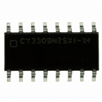
CY2309NZSXI-1H Cypress Semiconductor Corp, CY2309NZSXI-1H Datasheet - Page 4

CY2309NZSXI-1H
Manufacturer Part Number
CY2309NZSXI-1H
Description
IC CLK BUFF 9OUT 133MHZ 16SOIC
Manufacturer
Cypress Semiconductor Corp
Type
Fanout Buffer (Distribution)r
Datasheet
1.CY2309NZSXC-1H.pdf
(10 pages)
Specifications of CY2309NZSXI-1H
Package / Case
16-SOIC (3.9mm Width)
Number Of Circuits
1
Ratio - Input:output
1:9
Differential - Input:output
No/No
Input
Clock
Output
Clock
Frequency - Max
133.3MHz
Voltage - Supply
3 V ~ 3.6 V
Operating Temperature
-40°C ~ 85°C
Mounting Type
Surface Mount
Frequency-max
133.3MHz
Number Of Outputs
9
Max Input Freq
133.33 MHz
Propagation Delay (max)
9.2 ns @ 3V to 3.6V
Supply Voltage (max)
3.6 V
Supply Voltage (min)
3 V
Maximum Operating Temperature
+ 85 C
Minimum Operating Temperature
- 40 C
Mounting Style
SMD/SMT
Lead Free Status / RoHS Status
Lead free / RoHS Compliant
Lead Free Status / RoHS Status
Lead free / RoHS Compliant, Lead free / RoHS Compliant
Other names
428-2205-5
CY2309NZSXI-1H
CY2309NZSXI-1H
Available stocks
Company
Part Number
Manufacturer
Quantity
Price
Company:
Part Number:
CY2309NZSXI-1H
Manufacturer:
CY
Quantity:
21
Company:
Part Number:
CY2309NZSXI-1HT-ND
Manufacturer:
CYPRESS
Quantity:
133
Maximum Ratings
Supply voltage to ground potential ...............–0.5 V to +7.0 V
DC input voltage ............................................–0.5 V to 7.0 V
Operating Conditions
Electrical Characteristics
Switching Characteristics
Document Number: 38-07182 Rev. *G
Notes
V
T
C
C
BUF_IN, OUTPUT [1:9] Operating frequency
t
V
V
I
I
V
V
I
t
t
t
t
PU
IL
IH
DD
3
4
5
6
1. BUF_IN input has a threshold voltage of V
2. Parameter is guaranteed by design and characterization. It is not 100% tested in production.
3. All parameters specified with loaded outputs.
Parameter
Parameter
A
DD
IL
IH
OL
OH
L
IN
Parameter
Input LOW voltage
Input HIGH voltage
Input LOW current
Input HIGH current
Output LOW voltage
Output HIGH voltage
Supply current
Duty cycle
Rise time
Fall time
Output to output skew
Propagation delay, BUF_IN
Rising edge to
Rising edge
[2]
[2]
Description
[2]
Supply voltage
(Ambient operating temperature) commercial
(Ambient operating temperature) industrial
Load capacitance, Fout < 100 MHz
Load capacitance,100 MHz < Fout < 133.33 MHz
Input capacitance
Power-up time for all VDDs to reach minimum specified
voltage (power ramps must be monotonic)
[2]
Name
= t
Output
2
t
for Commercial and Industrial Temperature Devices
[1]
[1]
1
[2]
[2]
[2]
DD
for Commercial and Industrial Temperature Devices
for Commercial and Industrial Temperature Devices
/2.
V
V
I
I
Unloaded outputs at 66.66 MHz
Measured at 1.4 V
Measured between 0.8 V and 2.0 V
Measured between 0.8 V and 2.0 V
All outputs equally loaded
Measured at V
OL
OH
IN
IN
Description
= 8 mA
= 0 V
= V
= –8 mA
DD
Test Conditions
Description
DD
/2
Storage temperature ................................ –65
Junction temperature................................................. 150
Static discharge voltage
(per MIL-STD-883, Method 3015) ........................... >2,000 V
40.0
Min
[3]
–
–
–
1
Min
0.05
2.0
2.4
Min
–40
3.0
DC
–
–
–
–
–
0
–
–
–
50.0
Typ
–
–
–
5
133.33
100.0
Max
50.0
Max
Max
60.0
1.50
1.50
0.8
0.4
250
3.6
32
9.2
70
85
30
15
50
–
–
7
CY2309NZ
C to +150
Page 4 of 10
MHz
Unit
Unit
Unit
mA
ms
A
A
pF
pF
pF
ns
ns
ps
ns
%
V
V
V
V
V
C
C
C
C
[+] Feedback


