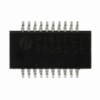
PI49FCT3805DQE Pericom Semiconductor, PI49FCT3805DQE Datasheet - Page 3

PI49FCT3805DQE
Manufacturer Part Number
PI49FCT3805DQE
Description
IC CLOCK DRIVER 3.3V 20-QSOP
Manufacturer
Pericom Semiconductor
Series
49FCTr
Type
Fanout Buffer (Distribution)r
Datasheets
1.PI49FCT3805DQE.pdf
(10 pages)
2.PI49FCT3805DQEX.pdf
(9 pages)
3.PI49FCT3805DQE.pdf
(9 pages)
Specifications of PI49FCT3805DQE
Number Of Circuits
2
Ratio - Input:output
1:5
Differential - Input:output
No/No
Input
CMOS, TTL
Output
CMOS
Frequency - Max
133MHz
Voltage - Supply
3 V ~ 3.6 V
Operating Temperature
-40°C ~ 85°C
Mounting Type
Surface Mount
Package / Case
20-QSOP
Frequency-max
133MHz
Number Of Outputs
10
Max Input Freq
166 MHz
Propagation Delay (max)
3 ns @ 3.3 V
Supply Voltage (max)
3.6 V
Supply Voltage (min)
3 V
Maximum Power Dissipation
500 mW
Maximum Operating Temperature
+ 85 C
Minimum Operating Temperature
- 40 C
Mounting Style
SMD/SMT
Operating Supply Voltage (max)
3.6V
Operating Temp Range
-40C to 85C
Propagation Delay Time
5.2ns
Operating Supply Voltage (min)
3V
Mounting
Surface Mount
Pin Count
20
Operating Supply Voltage (typ)
3.3V
Package Type
QSOP
Quiescent Current
30uA
Power Dissipation
500mW
Input Frequency
166MHz
Operating Temperature Classification
Industrial
Lead Free Status / RoHS Status
Lead free / RoHS Compliant
Available stocks
Company
Part Number
Manufacturer
Quantity
Price
Company:
Part Number:
PI49FCT3805DQE
Manufacturer:
PER
Quantity:
274
Company:
Part Number:
PI49FCT3805DQE
Manufacturer:
PERICOM
Quantity:
497
Company:
Part Number:
PI49FCT3805DQE
Manufacturer:
PERICOM
Quantity:
266
Part Number:
PI49FCT3805DQE
Manufacturer:
PERICOM
Quantity:
20 000
Company:
Part Number:
PI49FCT3805DQEX
Manufacturer:
PERICOM
Quantity:
7
Electrical Specifications
Maximum Ratings
DC Electrical Characteristics
1. For Max. or Min. conditions, use appropriate value specified under Electrical Characteristics for the applicable device type.
2. Typical values are at V
3. V
4. This parameter is determined by device characterization but is not production tested.
5. Not more than one output should be shorted at one time. Duration of the test should not exceed one second.
V
V
V
V
I
I
I
I
V
I
I
I
V
Symbol
OZH
OZL
ODH
ODL
OS
IH
IL
Storage Temperature ................................................................–65°C to +150°C
Ambient Temperature with Power Applied .......................... –40°C to +85°C
Supply Voltage to Ground Potential (Inputs & Vcc Only) ....–0.5V to +7.0V
Supply Voltage to Ground Potential (Outputs & I/O Only) .–0.5V to +7.0V
DC Input Voltage ........................................................................–0.5V to +7.0V
DC Output Current ................................................................................ 120 mA
Power Dissipation ........................................................................................0.5W
OH
OL
IH
IL
IK
H
OH
= V
10-0117
CC
– 0.6V at rated current.
Output High Voltage
V
Output Low Voltage
V
Input High Voltage
Input Low Voltage
Input High Current
Input Low Current
High Impedance Output
Current
High Impedance Output
Current
Clamp Diode Voltage
Output HIGH Current
Output LOW Current
Short Circuit
Input Hysteresis
Parameter
CC
CC
= 3.0V, V
= 3.0V, V
CC
= 3.3V, +25°C ambient and maximum loading.
(Above which the useful life may be impaired. For user guidelines, not tested.)
(5)
IN
IN
Current
= V
= V
IL
IL
or V
or V
(T
A
IH
IH
= –40°C to +85°C, V
Test Condition
V
V
V
V
Guaranteed Logic
HIGH level
Guaranteed Logic
LOW level
V
V
V
All outputs Disabled
V
All outputs Disabled
V
V
V
V
V
V
CC
CC
CC
CC
CC
CC
CC
OUT
OUT
OUT
OUT
CC
IN
IN
= V
= V
= Min.,
= Min.,
= Max
= Max
= Max.,
= Max.,
= Min., I
= Max., V
= 3.3V, V
= 1.5V
= 3.3V, V
= 1.5V
IH
IH
or V
or V
(4)
(4)
IN
OUT
CC
IL
IL
IN
IN
= -18mA
(1)
=V
= V
= 3.3V ±0.3V)
= GND
3
IL
IL
or V
or V
I
I
I
I
I
Input Pins
Input Pins
V
(Input Pins)
V
(Input & I/O
Pins)
V
V
V
V
OH
OH
OL
OL
OL
(5)
OUT
OUT
OUT
OUT
IN
IN
IH,
IH,
= 0.1mA
= 16mA
= 24mA
= -0.1mA
= -8mA
= V
= GND
= V
= GND
= V
= GND
CC
Note:
Stresses greater than those listed under MAXIMUM RAT-
INGS may cause permanent damage to the device. This is
a stress rating only and functional operation of the device
at these or any other conditions above those indicated in
the operational sections of this specification is not implied.
Exposure to absolute maximum rating conditions for
extended periods may affect reliability.
CC
CC
PI49FCT3805/PI49FCT3806
3.3V Fast CMOS Buffer/Clock Driver
V
2.0
-0.5
-1
-1
-1
-1
-35
50
-60
Min.
2.4 (3)
CC
www.pericom.com
-0.2
-
3.0
-
0.2
0.3
-0.7
-86
168
-135
150
Typ.
PS7007J
0.2
0.4
0.5
5.5
0.8
1
1
1
1
-1.2
-110
200
-240
Max.
Units
V
µA
V
mA
mV
02/16/10


