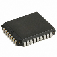
CY7B991-2JC Cypress Semiconductor Corp, CY7B991-2JC Datasheet

CY7B991-2JC
Specifications of CY7B991-2JC
Available stocks
Related parts for CY7B991-2JC
CY7B991-2JC Summary of contents
Page 1
... TTL or CY7B992 CMOS). Each output can be hardwired to one of nine delay or function configurations. Delay increments of 0.7 to 1.5 ns are deter- mined by the operating frequency with outputs able to skew time units from their nominal “ ...
Page 2
... FB is undivided. The frequency of the REF and FB inputs will be f frequency multiplication by using a divided output as the FB input. 3. When the FS pin is selected HIGH, the REF input must not transition upon power-up until V CY7B991 CY7B992 [1] Output Functions 1F0, 2F0, 1Q0, 1Q1, ...
Page 3
... Test Mode The TEST input is a three-level input. In normal system oper- ation, this pin is connected to ground, allowing the CY7B991/CY7B992 to operate as explained briefly above (for testing purposes, any of the three-level inputs can have a re- movable jumper to ground tied LOW through a 100 resistor. This will allow an external tester to change the state of these pins ...
Page 4
... CC before all datasheet limits are achieved. 8. CY7B991 should be tested one output at a time, output shorted for less than one second, less than 10% duty cycle. Room temperature only. CY7B992 outputs should not be shorted to GND. Doing so may cause permanent damage. 9. Total output current per output pair can be approximated by the following expression that includes device current plus load current: CY7B991 [(4 + 0.11F) + [((835 – ...
Page 5
... Applies to REF and FB inputs only. Tested initially and after any design or process changes that may affect these parameters. AC Test Loads and Waveforms 5V R1=130 R1 R2= (Includes fixture and probe capacitance 7B991–4 TTL AC Test Load (CY7B991 R1=100 R2=100 (Includes fixture and probe capacitance 7B991–6 CMOS AC Test Load (CY7B992) Document #: 38-07138 Rev ...
Page 6
... Jitter Note: 13. Test measurement levels for the CY7B991 are TTL levels (1.5V to 1.5V). Test measurement levels for the CY7B992 are CMOS levels (V conditions assume signal transition times less and output loading as shown in the AC Test Loads and Waveforms unless otherwise specified. 14. Guaranteed by statistical correlation. Tested initially and after any design or process changes that may affect these parameters. ...
Page 7
... RMS [14] Peak-to-Peak CY7B991 CY7B992 CY7B992–5 Max. Min. Typ. Max [15 5.0 5.0 See Table 1 0.25 0.1 0.25 0.5 0.25 0.5 0.7 ...
Page 8
... RMS [14] Peak-to-Peak CY7B991 CY7B992 CY7B992–7 Max. Min. Typ. Max [15 5.0 5.0 See Table 1 0.25 0.1 0.25 0.75 0.3 0.75 1.0 ...
Page 9
... AC Timing Diagrams t REF t RPWH REF SKEWPR, t SKEW0,1 OTHER Q INVERTED Q t SKEW3,4 REF DIVIDED SKEW1,3, 4 REF DIVIDED BY 4 Document #: 38-07138 Rev RPWL t ODCV t ODCV t SKEWPR, t SKEW0,1 t SKEW2 t SKEW2 t SKEW3,4 t SKEW3,4 t SKEW2,4 CY7B991 CY7B992 t JR 7B991–8 Page ...
Page 10
... FB and setting 1F0 = 1F1 = GND, LOAD LOAD LOAD LOAD Z 0 7B991–9 LOAD Z 0 LOAD Z 0 LOAD Z 0 LOAD Z 0 7B991–10 , and –t are defined relative to output U U between REF and 3Qx can be U CY7B991 CY7B992 ) when using U Page ...
Page 11
... It can multiply by two and four or divide by two (and four) at the same time that it is shifting its outputs over a wide range or maintaining zero skew between selected outputs. CY7B991 CY7B992 frequency outputs without concern for ris- REF ...
Page 12
... TEST Figure 8 shows the CY7B991/992 connected in series to con- struct a zero-skew clock distribution tree between boards. De- lays of the downstream clock buffers can be programmed to compensate for the wire length (i.e., select negative skew equal to the wire delay) necessary to connect them to the mas- Document #: 38-07138 Rev ...
Page 13
... Ordering Information Accuracy (ps) Ordering Code 250 CY7B991–2JC 500 CY7B991–5JC CY7B991–5JI 750 CY7B991–7JC CY7B991–7JI CY7B991–7LMB 250 CY7B992–2JC 500 CY7B992–5JC CY7B992–5JI 750 CY7B992–7JC CY7B992–7JI CY7B992–7LMB MILITARY SPECIFICATIONS Group A Subgroup Testing DC Characteristics ...
Page 14
... The inclusion of Cypress Semiconductor products in life-support systems application implies that the manufacturer assumes all risk of such use and in doing so indemnifies Cypress Semiconductor against all charges. 32-Lead Plastic Leaded Chip Carrier MIL-STD-1835 C-12 CY7B991 CY7B992 Page ...
Page 15
... Document Title: CY7B991/CY7B992 Programmable Skew Clock Buffer (PSCB) Document Number: 38-07138 Issue REV. ECN NO. Date ** 110247 12/19/01 Document #: 38-07138 Rev. ** Orig. of Change SZV Change from Spec number: 38-00513 to 38-07138 CY7B991 CY7B992 Description of Change Page ...


