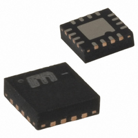
SY56020XRMG Micrel Inc, SY56020XRMG Datasheet - Page 5

SY56020XRMG
Manufacturer Part Number
SY56020XRMG
Description
IC CLOCK FANOUT BUFFER 1:4 16MLF
Manufacturer
Micrel Inc
Series
Precision Edge®r
Type
Fanout Buffer (Distribution)r
Datasheet
1.SY56020XRMG.pdf
(10 pages)
Specifications of SY56020XRMG
Number Of Circuits
1
Ratio - Input:output
1:4
Differential - Input:output
Yes/Yes
Input
CML, LVDS, LVPECL
Output
CML
Frequency - Max
4.5GHz
Voltage - Supply
2.375 V ~ 2.625 V
Operating Temperature
-40°C ~ 85°C
Mounting Type
Surface Mount
Package / Case
16-MLF®, QFN
Frequency-max
4.5GHz
Lead Free Status / RoHS Status
Lead free / RoHS Compliant
Other names
576-3698-5
SY56020XRMG
SY56020XRMG
Available stocks
Company
Part Number
Manufacturer
Quantity
Price
Company:
Part Number:
SY56020XRMG
Manufacturer:
Maxim
Quantity:
42
Micrel, Inc.
CML Outputs DC Electrical Characteristics
V
V
V
Three Level EQ Input DC Electrical Characteristics
V
AC Electrical Characteristics
V
V
V
Notes:
6.
7.
8.
9.
10. Random jitter is additive jitter.
11. Deterministic jitter is measured with 2
February 2010
Symbol
V
V
V
R
Symbol
V
V
I
I
Symbol
f
t
t
t
t
CCO
CCO
CC
CC
CCO
CCO
CC
IH
IL
MAX
PD
Skew
Jitter
R
OH
OUT
DIFF_OUT
IH
IL
OUT
t
F
= 2.375V to 2.625V; T
The circuit is designed to meet the DC specifications shown in the above table after thermal equilibrium has been established.
Output-to-Output skew is the difference in time between both outputs under identical input transition, temperature and power supply
Part-to-part skew is defined for two parts with identical power supply voltages at the same temperature and no skew at the edges at the
respective inputs.
Propagation delay is measured with no attenuating transmission line connected to the input.
= 2.375V to 2.625V; T
= 2.375V to 2.625V; T
= 1.14V to 1.26V R
= 1.7V to 1.9V, 2.375V to 2.625V, R
= 1.14V to 1.26V R
= 1.7V to 1.9V, 2.375V to 2.625V, R
Parameter
Output HIGH Voltage
Output Voltage Swing
Differential Output Voltage Swing
Output Source Impedance
Parameter
Input HIGH Voltage
Input LOW Voltage
Input HIGH Current
Input LOW Current
Parameter
Maximum Frequency
Propagation Delay (IN-to-Q)
Output-to-Output Skew
Part-to-Part Skew
Data Random Jitter
Data Deterministic Jitter
Output Rise/Fall Time
(20% to 80%)
Duty Cycle
L
L
= 50Ω to V
A
= 50Ω to V
A
A
= –40°C to +85°C, unless otherwise stated.
= –40°C to +85°C, unless otherwise stated.
= –40°C to +85°C, unless otherwise stated.
23
–1 PRBS pattern.
CCO
CCO
.
.
L
L
= 50Ω to V
= 50Ω to V
Condition
Condition
Condition
NRZ Data
Note 10
R
See Figure 3a
See Figure 3b
V
V
V
Note 7, Figure 1
Note 8
Note 9
Note 11
At full output swing.
Differential I/O
IH
IL
OUT
L
= 50Ω to V
= GND
= V
> 200mV (Clock)
CC
CCO
CCO
CCO
or 100Ω across the outputs.
or 100Ω across the outputs.
(6)
5
(6)
V
V
CC
CC
-480
Min
300
600
Min
Min
120
6.4
4.5
-0.020
45
30
45
hbwhelp@micrel.com
0
-0.3
V
CC
Typ
Typ
Typ
390
780
200
-0.010
50
60
3
or (408) 955-1690
M9999-020210-A
V
EE
Max
Max
Max
V
475
950
V
400
300
100
100
0.8
55
15
10
55
SY56020XR
+0.3
CC
CC
Units
Units
Units
ps
Gbps
GHz
ps
mV
mV
µA
µA
ps
ps
ps
ps
%
V
Ω
V
V
RMS
PP


