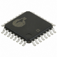
CY29948AXI Cypress Semiconductor Corp, CY29948AXI Datasheet - Page 2

CY29948AXI
Manufacturer Part Number
CY29948AXI
Description
IC CLK BUFF 1:12 200MHZ 32TQFP
Manufacturer
Cypress Semiconductor Corp
Type
Fanout Buffer (Distribution), Multiplexerr
Datasheet
1.CY29948AXC.pdf
(7 pages)
Specifications of CY29948AXI
Package / Case
32-TQFP
Number Of Circuits
1
Ratio - Input:output
2:12
Differential - Input:output
Yes/No
Input
LVCMOS, LVPECL, LVTTL
Output
LVCMOS, LVTTL
Frequency - Max
200MHz
Voltage - Supply
2.375 V ~ 3.63 V
Operating Temperature
-40°C ~ 85°C
Mounting Type
Surface Mount
Frequency-max
200MHz
Minimum Operating Temperature
- 40 C
Mounting Style
SMD/SMT
Number Of Clock Inputs
2
Output Logic Level
LVCMOS, LVTTL
Supply Voltage (max)
3.63 V
Supply Voltage (min)
2.375 V
Maximum Operating Temperature
+ 85 C
Lead Free Status / RoHS Status
Lead free / RoHS Compliant
Available stocks
Company
Part Number
Manufacturer
Quantity
Price
Company:
Part Number:
CY29948AXI
Manufacturer:
Cypress Semiconductor Corp
Quantity:
135
Company:
Part Number:
CY29948AXI
Manufacturer:
CY
Quantity:
195
Company:
Part Number:
CY29948AXI
Manufacturer:
Cypress Semiconductor Corp
Quantity:
10 000
Company:
Part Number:
CY29948AXIT
Manufacturer:
Cypress Semiconductor Corp
Quantity:
10 000
Pin Description
Output Enable/Disable
The CY29948 features a control input to enable or disable the
outputs. This data is latched on the falling edge of the input clock.
When SYNC_OE is asserted LOW, the outputs are disabled in a
LOW state. When SYNC_OE is set HIGH, the outputs are
enabled as shown in
Note
Document Number: 38-07288 Rev. *D
17, 19, 21, 23,
10, 14, 18, 22,
1. PD = Internal pull-down, PU = Internal pull-up.
25, 27, 29, 31
8, 12, 16, 20,
9, 11, 13, 15,
24, 28, 32
26, 30
Pin
3
4
2
1
5
6
7
SYNC_OE
TCLK
PECL_CLK#
PECL_CLK
TCLK_SEL
SYNC_OE
Q
Q(11:0)
Figure
VDDC
Name
TCLK
[1]
VDD
VSS
TS#
1.
VDDC
PWR
Figure 1. SYNC_OE Timing Diagram
I, PU PECL Input Clock
I, PD PECL Input Clock
I, PU External Reference/Test Clock Input
I, PU Clock Select Input. When LOW, PECL clock is selected. When HIGH
I, PU Output Enable Input. When asserted HIGH, the outputs are enabled.
I, PU Three-state Control Input. When asserted LOW, the output buffers
I/O
O
Clock Outputs
TCLK is selected.
When set LOW the outputs are disabled in a LOW state.
are three-stated. When set HIGH, the output buffers are enabled.
2.5V or 3.3V Power Supply for Output Clock Buffers
2.5V or 3.3V Power Supply
Common Ground
Description
CY29948
Page 2 of 7
[+] Feedback


