LMK01010ISQE/NOPB National Semiconductor, LMK01010ISQE/NOPB Datasheet
LMK01010ISQE/NOPB
Specifications of LMK01010ISQE/NOPB
LMK01010ISQE
LMK01010ISQETR
Available stocks


Related parts for LMK01010ISQE/NOPB

LMK01010ISQE/NOPB Summary of contents
Page 1
... Medical Imaging ■ Wired Communications ■ Test and Measurement ■ Military / Aerospace System Diagram TRI-STATE® registered trademark of National Semiconductor Corporation. © 2009 National Semiconductor Corporation LMK01000 Family Features ■ additive jitter (100 MHz) ■ Dual clock inputs ■ Programmable output channels (0 to 1600 MHz) ■ ...
Page 2
Functional Block Diagram Connection Diagram www.national.com 48-Pin LLP Package 2 30042801 30042802 ...
Page 3
Pin Descriptions Pin # 9,10 13, 16, 19, 22, 26, Vcc1, Vcc2, Vcc3, Vcc4, Vcc5, Vcc6, Vcc7, 30, 31, 33, 37, 40, 43, 46 Vcc8, Vcc9, Vcc10, Vcc11, Vcc12, Vcc13, Vcc14 4 5 ...
Page 4
... Absolute Maximum Ratings If Military/Aerospace specified devices are required, please contact the National Semiconductor Sales Office/ Distributors for availability and specifications. Parameter Power Supply Voltage Input Voltage Storage Temperature Range Lead Temperature (solder 4 s) Junction Temperature Recommended Operating Conditions Parameter Ambient Temperature Power Supply Voltage Note 1: " ...
Page 5
Symbol Parameter Delay Maximum Allowable Delay(Note CLKout Allowable divide range. (Note that 1 is Divide CLKoutX the only allowable odd divide value) Jitter Additive RMS Jitter (Note ADD Noise Floor Divider Noise Floor(Note t CLKoutX to CLKoutY (Note SKEW V ...
Page 6
Symbol Parameter Jitter Additive RMS Jitter(Note ADD Noise Floor Divider Noise Floor(Note t CLKoutX to CLKoutY (Note SKEW V Output High Voltage OH V Output Low Voltage OL V Differential Output Voltage OD V High-Level Input Voltage IH V Low-Level ...
Page 7
Symbol Parameter V High-Level Input Voltage IH V Low-Level Input Voltage IL I High-Level Input Current IH I Low-Level Input Current IL t Data to Clock Set Up Time CS t Data to Clock Hold Time CH t Clock Pulse ...
Page 8
Typical Performance Characteristics LVDS Differential Output Voltage (V LVDS Output Noise Floor Delay Noise Floor (Adds to Output Noise Floor) www.national.com ) LVPECL Differential Output Voltage (V OD 30042807 LVPECL Output Noise Floor 30042809 30042811 30042808 30042810 ...
Page 9
... LVDS receiver. To ensure such conditions, we recommend the usage of LVDS receivers without fail-safe or internal input bias such as National Semiconductor's DS90LV110T. The LMK01000 family LVDS drivers provide the adequate DC bias for the LVDS receiver. We recommend AC coupling when using LVDS receivers with fail-safe or internal input bias ...
Page 10
General Programming Information The LMK01000 family device is programmed using several 32-bit registers. The registers consist of a data field and an address field. The last 4 register bits, ADDR[3:0] form the ad- dress field. The remaining 28 bits ...
Page 11
CLKout0 CLKout1 CLKout2 _EN _EN _EN RESET Register CLKout3 CLKout4 CLKout5 CLKout6 _EN _EN _EN _EN 11 CLKout7 _EN POWERDOWN EN_CLKout _Global CLKin _SELECT www.national.com ...
Page 12
REGISTER Registers R0 through R7 control the eight clock outputs. Reg- ister R0 controls CLKout0, Register R1 controls CLKout1, and so on. There is one additional bit in register R0 called RESET. Default Bit Name Bit ...
Page 13
CLKoutX_EN bit -- Clock Output Enables These bits control whether an individual clock output is en- abled or not. If the EN_CLKout_Global bit is set to zero or if GOE pin is held low, all CLKoutX_EN bit states will ...
Page 14
Application Information 3.1 SYSTEM LEVEL DIAGRAM The following shows a typical application for a LMK01000 family device. In this setup the clock may be divided, skewed, and redistributed. www.national.com FIGURE 1. Typical Application 14 30042870 ...
Page 15
CURRENT CONSUMPTION / POWER DISSIPATION CALCULATIONS (Vcc = 3 25° Block Condition Core Current All outputs disabled. Includes input buffer currents. Low clock buffer The low clock buffer is enabled anytime one of CLKout0 ...
Page 16
... Figure 3. To ensure proper LVDS operation when DC cou- pling it is recommend to use LVDS receivers without fail-safe or internal input bias such as National Semiconductor's DS90LV110T. The LVDS driver will provide the DC bias level for the LVDS receiver. For operation with LMK01000 family LVDS drivers it is recommend to use AC coupling with LVDS receivers that have an internal DC bias voltage ...
Page 17
FIGURE 5. Differential LVPECL Operation, DC Coupling, Thevenin Equivalent FIGURE 6. Differential LVDS Operation, AC Coupling LVPECL drivers require a DC path to ground. When AC cou- pling an LVPECL signal use 120 Ω emitter resistors close to the LVPECL ...
Page 18
Figure 9 for Vcc = 3.3 V. FIGURE 8. Single-Ended LVPECL Operation, DC Coupling FIGURE 9. Single-Ended LVPECL Operation, DC Coupling, Thevenin Equivalent When AC ...
Page 19
FIGURE 13. Recommended OSCin Power for Operation with a Sine Wave Input 3.6 MORE THAN EIGHT OUTPUTS WITH AN LMK01000 FAMILY DEVICE The LMK01000 family device can be used in conjunction with a LMK02000, LMK03000, LMK04000, or even another LMK01000 ...
Page 20
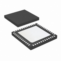
Physical Dimensions Order Number LMK01000ISQX LMK01000ISQ LMK01000ISQE LMK01010ISQX LMK01010ISQ LMK01010ISQE LMK01020ISQX LMK01020ISQ LMK01020ISQE www.national.com inches (millimeters) unless otherwise noted Leadless Leadframe Package (Bottom View) 48 Pin LLP (SQA48A) Package Package Marking K01000 I K01000 I K01000 I K01010 I K01010 ...
Page 21
Notes 21 www.national.com ...
Page 22
... For more National Semiconductor product information and proven design tools, visit the following Web sites at: Products Amplifiers www.national.com/amplifiers Audio www.national.com/audio Clock and Timing www.national.com/timing Data Converters www.national.com/adc Interface www.national.com/interface LVDS www.national.com/lvds Power Management www.national.com/power Switching Regulators www.national.com/switchers LDOs www.national.com/ldo LED Lighting www ...