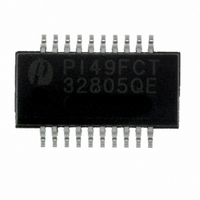
PI49FCT32805QE Pericom Semiconductor, PI49FCT32805QE Datasheet - Page 2

PI49FCT32805QE
Manufacturer Part Number
PI49FCT32805QE
Description
IC 2X1:5 CLOCK DRIVER 20-QSOP
Manufacturer
Pericom Semiconductor
Series
49FCTr
Type
Fanout Buffer (Distribution)r
Datasheet
1.PI49FCT32805QE.pdf
(7 pages)
Specifications of PI49FCT32805QE
Number Of Circuits
2
Ratio - Input:output
1:5
Differential - Input:output
No/No
Input
CMOS
Output
CMOS
Frequency - Max
133MHz
Voltage - Supply
2.97 V ~ 3.63 V
Operating Temperature
-40°C ~ 85°C
Mounting Type
Surface Mount
Package / Case
20-QSOP
Frequency-max
133MHz
Number Of Outputs
10
Operating Supply Voltage (max)
3.63V
Operating Temp Range
-40C to 85C
Propagation Delay Time
5.2ns
Operating Supply Voltage (min)
2.97V
Mounting
Surface Mount
Pin Count
20
Operating Supply Voltage (typ)
3.3V
Package Type
QSOP
Quiescent Current
30uA
Power Dissipation
500mW
Input Frequency
133MHz
Operating Temperature Classification
Industrial
Max Input Freq
133 MHz
Propagation Delay (max)
3 ns @ 3.3V
Supply Voltage (max)
3.63 V
Supply Voltage (min)
2.97 V
Maximum Power Dissipation
500 mW
Maximum Operating Temperature
+ 85 C
Minimum Operating Temperature
- 40 C
Mounting Style
SMD/SMT
Lead Free Status / RoHS Status
Lead free / RoHS Compliant
Lead Free Status / RoHS Status
Lead free / RoHS Compliant, Compliant
Available stocks
Company
Part Number
Manufacturer
Quantity
Price
Company:
Part Number:
PI49FCT32805QE
Manufacturer:
PERICOM
Quantity:
886
Part Number:
PI49FCT32805QEX
Manufacturer:
PERICOM
Quantity:
20 000
Capacitance
Note:
1.
Maximum Ratings
DC Electrical Characteristics
Notes:
1.
2.
3.
4.
Storage Temperature .......................................................... –65°C to +150°C
Ambient Temperature with Power Applied ......................... –40°C to +85°C
Supply Voltage to Ground Potential (Inputs & V
Supply Voltage to Ground Potential (Outputs & I/O Only).. –0.5V to +4.6V
DC Input Voltage .................................................................. –0.5V to +4.6V
DC Output Current............................................................................ 120 mA
Power Dissipation ................................................................................. 0.5W
Symbol
Parameters
V
I
V
I
V
V
V
I
OZH
I
I
I
OZL
I
R
This parameter is determined by device characterization.
For Max or Min conditions, use appropriate value specified under Electrical Characteristics for the applicable device type.
V
This parameter is guaranteed by device characterization.
Not more than one output should be shorted at one time. Duration of the test should not exceed one second.
OH
OL
OS
OH
IH
OL
IL
IH
IK
IL
S
OH
C
C
OUT
= V
IN
Parameter
Output High Voltage
V
Output Low Voltage
V
Input High Voltage
Input Low Voltage
Input High Current
Input Low Current
High Impedance Output
Current
High Impedance Output
Current
Clamp Diode Voltage
Output HIGH Current
Output LOW Current
Short Circuit Current
Internal Series Resistor
CC
CC
CC
(1)
– 0.6V at rated current.
(T
= 3.0V, V
= 3.0V, V
A
= 25°C, f = 1 MHz)
Description
Input Capacitance
Output Capacitance
IN
IN
= V
= V
IL
IL
(3)
(4)
(3)
or V
or V
(T
A
IH
IH
= –40°C to +85°C, V
Test Condition
I
I
V
V
V
All outputs Disabled
V
All outputs Disabled
V
V
V
V
OH
OL
CC
CC
CC
CC
CC
OUT
OUT
CC
CC
= +12mA
= -8mA
= Max., V
= Max., V
= Max.,
= Max.,
= Min., I
= Max., V
= 1.5V, V
= 1.5V, V
Only)... –0.5V to +4.6V
IN
IN
IN
OUT
(1)
IN
IN
= -18mA
CC
= V
= GND
=V
= V
2
= GND
Test Conditions
V
V
= 3.3V ± 10%)
CC
IL
IN
OUT
IL
or V
= 0V
V
V
or V
OUT
OUT
= 0V
IH,
IH,
= V
= GND
V
V
CC
CC
CC
Note:
Stresses greater than those listed under MAXIMUM RAT-
INGS may cause permanent damage to the device. This is
a stress rating only and functional operation of the device
at these or any other conditions above those indicated in
the operational sections of this specification is not implied.
Exposure to absolute maximum rating conditions for ex-
tended periods may affect reliability.
= 3.3V
= 3.3V
3.3V, 2 x 1:5 CMOS Clock Driver
2.4
Min.
-0.5
2.0
-25
-50
25
(2)
Typ
Typ.
-100
-0.9
-55
3.0
0.4
45
20
Max.
PI49FCT32805
4
6
V
Max.
CC
-180
-1.2
-80
0.5
0.8
90
PS8494C
-1
-1
1
1
-0.2
Units
pF
Units
mA
12/19/05
µA
Ω
V
V


