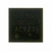
SI5330C-A00207-GM Silicon Laboratories Inc, SI5330C-A00207-GM Datasheet - Page 9

SI5330C-A00207-GM
Manufacturer Part Number
SI5330C-A00207-GM
Description
IC BUFFER HCSL DIFF 4OUT 24-QFN
Manufacturer
Silicon Laboratories Inc
Type
Fanout Buffer (Distribution), Translatorr
Datasheet
1.SI5330C-A00207-GM.pdf
(20 pages)
Specifications of SI5330C-A00207-GM
Number Of Circuits
1
Ratio - Input:output
1:4
Differential - Input:output
Yes/Yes
Input
CML, CMOS, HCSL, HSTL, LVDS, LVPECL, LVTTL, SSTL
Output
HCSL
Frequency - Max
250MHz
Voltage - Supply
1.71 V ~ 3.63 V
Operating Temperature
-40°C ~ 85°C
Mounting Type
Surface Mount
Package / Case
24-QFN
Frequency-max
250MHz
Lead Free Status / RoHS Status
Lead free / RoHS Compliant
Lead Free Status / RoHS Status
Lead free / RoHS Compliant, Lead free / RoHS Compliant
Other names
336-1551-5
Available stocks
Company
Part Number
Manufacturer
Quantity
Price
Company:
Part Number:
SI5330C-A00207-GM
Manufacturer:
TI
Quantity:
1 322
3. Functional Description
The Si5330 is a low-jitter, low-skew fanout buffer
optimized for high-performance PCB clock distribution
applications. The device produces four differential or
eight single-ended, low-jitter output clocks from a single
input clock. The input can accept either a single-ended
or a differential clock allowing the device to function as a
clock level translator.
3.1. V
The core V
and independent supply pins allowing the core supply to
operate at a different voltage than the I/O voltage levels.
The V
which operates from 1.8, 2.5, or 3.3 V. Using a lower
supply voltage helps minimize the device’s power
consumption. The V
output signal levels and must be set at a voltage level
compatible with the output signal format.
3.2. Loss Of Signal Indicator (LOS)
The input is monitored for a valid clock signal using an
LOS circuit that monitors input clock edges and
declares an LOS condition when signal edges are not
detected over a 5 μs observation period. The LOS pin is
asserted “low” when valid clock is present. A “high” level
on the LOS pin indicates a loss of signal (LOS). The
LOS pin must be pulled to VDD as shown in Figure 2.
Figure 2. LOS Indicator with External Pull-Up
LOS
IN
0
1
DD
Valid Clock
No Clock
DD
1k
supply powers the core functions of the device,
V
DD
and V
DD
and output V
Si5330
DDO
Control
DDO
Supplies
supply pins are used to set the
DDO
supplies have separate
CLK0
CLK1
CLK3
V
V
V
CLK2
V
DDO0
DDO1
DDO2
DDO3
Rev. 0.35
3.3. Output Enable (OEB)
The output enable (OEB) pin allows disabling or
enabling of the outputs clocks (CLK0-CLK3). The output
enable is logically controlled to ensure that no glitches
or runt pulses are generated at the output as shown in
Figure 3.
All outputs are enabled when the OEB pin is connected
to ground or below the V
Connecting the OEB pin to VDD or above the V
will disable the outputs. Both V
in Table 7. All outputs are forced to a logic “low” when
disabled. The OEB pin is 3.3 V tolerant.
3.4. Input Signals
The Si5330 can accept single-ended and differential
input clocks. See “AN408: Termination Options for Any-
Frequency, Any-Output Clock Generators and Clock
Buffers—Si5338, Si5334, Si5330” for details on
connecting a wide variety of signals to the Si5330
inputs.
3.5. Output Driver Formats
The Si5330 supports single-ended output formats of
CMOS, SSTL, and HSTL and differential formats of
LVDS, LVPECL, and HCSL. It is normally required that
the LVDS driver be dc-coupled to the 100 termination
at the receiver end. If your application requires an ac-
coupled 100 load, contact the applications team for
advice. See AN408 for additional information on the
terminations for these driver types.
3.6. Input and Output Terminations
See AN408 for detailed information.
4. Ordering the Si5330
The Si5330 can be ordered to meet the requirements of
the most commonly-used input and output signal types,
such as CMOS, SSTL, HSTL, LVPECL, LVDS, and
HSCL.
Diagrams,” on page 2 and Table 10, “Order Numbers
and Device Functionality,” on page 14 for specific
ordering information.
CLKn
OEB
IN
Figure 3. OEB Glitchless Operation
See
Enable
Figure 1,
Disable
“Si5330
IL
IL
voltage for this pin.
Disable
and V
Functional
IH
Si5330
are specified
Enable
IH
Block
level
9


