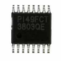
PI49FCT3803QE Pericom Semiconductor, PI49FCT3803QE Datasheet - Page 3

PI49FCT3803QE
Manufacturer Part Number
PI49FCT3803QE
Description
IC CLOCK BUFFER 1:5/1:7 16-QSOP
Manufacturer
Pericom Semiconductor
Series
49FCTr
Type
Fanout Buffer (Distribution)r
Datasheet
1.PI49FCT3803QE.pdf
(6 pages)
Specifications of PI49FCT3803QE
Number Of Circuits
1
Ratio - Input:output
1:7
Differential - Input:output
No/No
Input
CMOS, TTL
Output
CMOS, TTL
Frequency - Max
156MHz
Voltage - Supply
3 V ~ 3.6 V
Operating Temperature
0°C ~ 70°C
Mounting Type
Surface Mount
Package / Case
16-QSOP
Frequency-max
156MHz
Number Of Outputs
7
Operating Supply Voltage (max)
3.6V
Operating Temp Range
-40C to 85C
Propagation Delay Time
2.5ns
Operating Supply Voltage (min)
3V
Mounting
Surface Mount
Pin Count
16
Operating Supply Voltage (typ)
3.3V
Package Type
QSOP
Quiescent Current
100nA
Power Dissipation
500mW
Input Frequency
156MHz
Operating Temperature Classification
Industrial
Lead Free Status / RoHS Status
Lead free / RoHS Compliant
Available stocks
Company
Part Number
Manufacturer
Quantity
Price
Part Number:
PI49FCT3803QEX
Manufacturer:
PERICOM
Quantity:
20 000
Power Supply Characteristics
Notes:
1.
2.
3.
Capacitance
Note:
1.
Switching Characteristics
Notes:
1.
2.
3.
4.
I
∆I
I
t
t
t
t
t
t
Parameters
R
PLH
PHL
sk(o)
sk(p)
sk(t)
DDQ
DD
Parameters
/t
DD
Parameters
For Max. or Min. conditions, use appropriate value specified under Electrical Characteristics for the applicable device.
Typical values are at V
Per TTL driven input (V
This parameter is determined by device characterization but is not production tested.
F
See test circuit and waveforms.
Minimum limits are guaranteed but not tested on Propagation Delays.
Skew measured at worse cast temperature (max. temp).
Identical conditions: loading, transitions, supply voltage, temperature, package type and speed grade.
(3)
(3)
(3)
C
C
OUT
IN
(1)
(T
Quiescent Power Supply Current
Supply Current per Inputs
@ TTL High
Dynamic Supply Current
A
CLKn Rise/Fall Time 0.8V ~ 2.0V
Propagation Delay BUF_IN to CLKn
Skew between two outputs of the same package (same
transition)
Skew between opposite transitions (t
output
Skew between two outputs of different packages
= 25°C, f = 1 MHz)
Input Capacitance
Output Capacitance
DD
IN
= 3.3V, +25°C ambient.
= V
Description
Description
DD
(V
– 0.6V); all other inputs at V
DD
= 3.3V ± 0.3V, T
Desciription
PHL
A
V
V
V
= 85°C)
DD
DD
DD
No load
- t
DD
Test Conditions
PLH
= Max.
= Max.
= 3.6V,
V
or GND.
V
OUT
3
IN
) of the same
Test Conditions
(4)
= 0V
= 0V
V
V
IN
IN
= V
= GND or V
100 MHz
125 MHz
156 Mhz
50 MHz
67 MHz
80 MHz
Test Conditions
DD
C
125 Mhz
-0.6V(3)
L
= 15pF,
Typ
3.0
—
DD
PI49FCT3802/PI49FCT3803
for Networking Applications
Min.
Min.
1.0
Max.
1:5/1:7 Clock Buffers
4
6
Typ.
121
0.1
47
43
56
66
81
97
Typ.
110
200
0.7
2.2
(2)
Max.
Max.
PS8559A
0.55
250
250
300
1.0
2.5
30
Units
pF
Units
Units
mA
09/14/04
µA
ns
ps
ns


