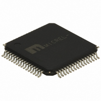
SY89468UHY Micrel Inc, SY89468UHY Datasheet - Page 3

SY89468UHY
Manufacturer Part Number
SY89468UHY
Description
IC BUFFER LVDS FANOUT 64-TQFP
Manufacturer
Micrel Inc
Type
Fanout Buffer (Distribution), Multiplexerr
Series
Precision Edge®r
Datasheet
1.SY89468UHY.pdf
(15 pages)
Specifications of SY89468UHY
Lead Free Status
Lead free
Number Of Circuits
1
Ratio - Input:output
2:20
Differential - Input:output
Yes/Yes
Input
CML, LVDS, PECL
Output
LVDS
Frequency - Max
1.5GHz
Voltage - Supply
2.375 V ~ 2.625 V
Operating Temperature
-40°C ~ 85°C
Mounting Type
Surface Mount
Package / Case
64-TQFP Exposed Pad, 64-eTQFP, 64-HTQFP, 64-VQFP
Frequency-max
1.5GHz
Number Of Clock Inputs
2
Mode Of Operation
Differential
Output Logic Level
LVDS
Operating Supply Voltage (min)
2.375V
Operating Supply Voltage (typ)
2.5V
Operating Supply Voltage (max)
2.625V
Package Type
TQFP EP
Operating Temp Range
-40C to 85C
Operating Temperature Classification
Industrial
Signal Type
CML/LVDS/PECL
Mounting
Surface Mount
Pin Count
64
Lead Free Status / RoHS Status
Compliant
Other names
576-2086
SY89468UHY
SY89468UHY
Available stocks
Company
Part Number
Manufacturer
Quantity
Price
Company:
Part Number:
SY89468UHY
Manufacturer:
MICREL
Quantity:
713
Pin Description
Truth Table
November 2008
Pin Number
1, 16, 23, 33
2, 3, 14, 15,
41, 48, 58
32, 40, 49
64, 63
62, 61
60, 59
57, 56
55, 54
53, 52
51, 50
47, 46
45, 44
43, 42
39, 38
37, 36
35, 34
31, 30
29, 28
27, 26
25, 24
22, 21
20, 19
18, 17
10, 11
4, 13
5, 12
6, 7
9
8
Exposed Pad
VREF-AC0
VREF-AC1
Pin Name
Q10, /Q10
Q11, /Q11
Q12, /Q12
Q13, /Q13
Q14, /Q14
Q15, /Q15
Q16, /Q16
Q17, /Q17
Q18, /Q18
Q19, /Q19
VT0, VT1
IN0, /IN0
IN1, /IN1
Q0, /Q0
Q1, /Q1
Q2, /Q2
Q3, /Q3
Q4, /Q4
Q5, /Q5
Q6, /Q6
Q7, /Q7
Q8, /Q8
Q9, /Q9
GND,
VCC
SEL
OE
IN0
X
X
Pin Function
Positive Power Supply: Bypass with 0.1µF||0.01µF low ESR capacitors as close to the V
pins as possible.
Differential Output Pairs: The output swing is typically 325mV. Used and unused outputs
must be terminated with 100Ω across the pair (Q, /Q). These differential LVDS outputs are a
logic function of the IN0, IN1, and SEL inputs. See “Truth Table” below.
Reference Voltage: These outputs bias to V
IN and /IN. Connect VREF-AC directly to the corresponding VT pin. Bypass with 0.01µF low
ESR capacitor to VCC. Due to limited drive capability, each VREF-AC pin is only intended to
drive its respective VT pin. Maximum sink/source current is ±0.5mA. See “Input Interface
Applications” subsection.
Input Termination Center-Tap: Each side of a differential input pair terminates to the VT pin.
The VT pin provides a center-tap for each input (IN, /IN) to a termination network for
maximum interface flexibility. See “Input Interface Applications” subsection.
Differential Inputs: These input pairs are the differential signal inputs to the device. These
inputs accept AC- or DC-coupled signals as small as 100mV. The input pairs internally
terminate to a VT pin through 50Ω. Each input has level shifting resistors of 3.72kΩ to VCC.
This allows a wide input voltage range from VCC to GND. See Figure 3, Simplified
Differential Input Stage for details. Note that when these inputs are left in an open state, the
FSI feature will override this input state and provide a valid state at the output. See
“Functional Description” subsection.
Ground. Exposed pad must be connected to a ground plane that is the same potential as
the ground pins.
Single-Ended Input: This TTL/CMOS input disables and enables the Q0-Q19 outputs. It is
internally connected to a 25kΩ pull-up resistor and will default to a logic HIGH state if left
open. When disabled, Q goes LOW and /Q goes HIGH. OE being synchronous, outputs will
be enabled/disabled following a rising and a falling edge of the input clock. V
Single-Ended Input: This single-ended TTL/CMOS-compatible input selects the inputs to the
multiplexer. Note that this input is internally connected to a 25kΩ pull-up resistor and will
default to logic HIGH state if left open. V
0
1
/IN0
X
X
1
0
Inputs
IN1
X
X
0
1
/IN1
X
X
3
1
0
SEL
0
0
1
1
TH
= V
CC
–1.2V. They are used for AC-coupling inputs
CC
Q
0
1
0
1
/2.
Outputs
hbwhelp@micrel.com
/Q
1
0
1
0
M9999-110308-D
or (408) 955-1690
TH
= V
CC
/2.
CC


