CY29942AXI Cypress Semiconductor Corp, CY29942AXI Datasheet - Page 3
CY29942AXI
Manufacturer Part Number
CY29942AXI
Description
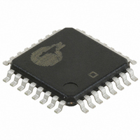
IC CLK BUFF 1:18 200MHZ 32LQFP
Manufacturer
Cypress Semiconductor Corp
Type
Fanout Buffer (Distribution)r
Datasheet
1.CY29942AXC.pdf
(9 pages)
Specifications of CY29942AXI
Package / Case
32-LQFP
Number Of Circuits
1
Ratio - Input:output
1:18
Differential - Input:output
No/No
Input
LVCMOS, LVTTL
Output
LVCMOS, LVTTL
Frequency - Max
200MHz
Voltage - Supply
2.375 V ~ 3.465 V
Operating Temperature
-40°C ~ 85°C
Mounting Type
Surface Mount
Frequency-max
200MHz
Number Of Outputs
18
Max Input Freq
200 MHz
Propagation Delay (max)
4.4 ns @ 2.5V or 3.8 ns @ 3.3V
Supply Voltage (max)
3.465 V
Supply Voltage (min)
2.375 V
Maximum Operating Temperature
+ 85 C
Minimum Operating Temperature
- 40 C
Mounting Style
SMD/SMT
Lead Free Status / RoHS Status
Lead free / RoHS Compliant
Lead Free Status / RoHS Status
Lead free / RoHS Compliant, Lead free / RoHS Compliant
Other names
428-2233
CY29942AXI
CY29942AXI
Available stocks
Company
Part Number
Manufacturer
Quantity
Price
Company:

Part Number:
CY29942AXI
Manufacturer:
CYPRESS
Quantity:
1 188
Company:
Part Number:
CY29942AXI
Manufacturer:
Cypress Semiconductor Corp
Quantity:
10 000
Company:
Part Number:
CY29942AXIT
Manufacturer:
Cypress Semiconductor Corp
Quantity:
10 000


Absolute Maximum Ratings
Maximum input voltage relative to V
Maximum input voltage relative to V
Storage temperature:.................................. –65 °C to 150 °C
Operating temperature: ................................ –40 °C to 85 °C
Maximum ESD protection............................................... 2 kV
Maximum power supply:................................................ 5.5 V
Maximum input current: ............................................. ±20 mA
DC Electrical Specifications
V
Document #: 38-07284 Rev. *F
V
V
I
I
V
V
I
I
Z
C
Notes
IL
IH
DDQ
DD
1. The voltage on any input or I/O pin cannot exceed the power pin during power-up.
2. Inputs have pull-up/pull-down resistors that effect input current.
3. Driving series or parallel terminated 50 (or 50 to V
DD
IL
IH
OL
OH
out
in
= 3.3 V ±5% or 2.5 V ±5% over the specified temperature range.
Parameter
Input low voltage
Input high voltage
Input low current
Input high current
Output low voltage
Output high voltage
Quiescent supply
current
Dynamic supply current V
Output impedance
Input capacitance
Description
SS
DD
[2]
:.............. V
:.............. V
[2]
[1]
[3]
[3]
DD
I
I
I
OE = V
CL = 15 pF
V
CL = 15 pF
V
CL = 15 pF
V
CL = 15 pF
V
V
OL
OH
OH
/2) transmission lines.
DD
DD
DD
DD
DD
DD
DD
SS
= 20 mA
= –20 mA, V
= –16 mA, V
= 3.3 V, Outputs at 150 MHz,
= 3.3 V, Outputs at 200 MHz,
= 2.5 V, Outputs at 150 MHz,
= 2.5 V, Outputs at 200 MHz,
= 3.3 V
= 2.5 V
– 0.3 V
+ 0.3 V
SS
Conditions
DD
DD
= 3.3 V
= 2.5 V
This device contains circuitry to protect the inputs against
damage due to high static voltages or electric field; however,
precautions should be taken to avoid application of any voltage
higher than the maximum rated voltages to this circuit. For proper
operation, I/O voltages should be constrained to the range:
V
Unused inputs must always be tied to an appropriate logic
voltage level (either V
SS
< V
I/O
< V
DD
Min
V
2.0
2.4
2.0
10
–
–
–
–
–
–
–
–
8
–
SS
SS
or V
Typ
285
335
200
240
DD
12
15
–
–
–
–
–
–
–
5
4
).
–200
Max
V
200
0.8
0.5
16
20
–
–
7
–
–
–
–
–
DD
CY29942
Unit
mA
mA
mA
mA
mA
Page 3 of 9
µA
µA
pF
V
V
V
V
V
[+] Feedback
Related parts for CY29942AXI
Image
Part Number
Description
Manufacturer
Datasheet
Request
R

Part Number:
Description:
Manufacturer:
Cypress Semiconductor Corp
Datasheet:
Part Number:
Description:
Manufacturer:
Cypress Semiconductor Corp
Datasheet:
Part Number:
Description:
Manufacturer:
Cypress Semiconductor Corp
Datasheet:
Part Number:
Description:
Manufacturer:
Cypress Semiconductor Corp
Datasheet:
Part Number:
Description:
Manufacturer:
Cypress Semiconductor Corp
Datasheet: