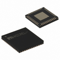
SY89465UMG TR Micrel Inc, SY89465UMG TR Datasheet

SY89465UMG TR
Specifications of SY89465UMG TR
576-1476-5
576-1476-5
SY89465UMG
Related parts for SY89465UMG TR
SY89465UMG TR Summary of contents
Page 1
... Precision Edge is a registered trademark of Micrel, Inc. MLF and MicroLeadFrame are trademarks of Amkor Technology, Inc. Micrel Inc. • 2180 Fortune Drive • San Jose, CA 95131 • USA • tel +1 (408) 944-0800 • fax + 1 (408) 474-1000 • http://www.micrel.com December 2005 Precision LVDS 1:10 Fanout with 2:1 Runt ...
Page 2
Typical Application December 2005 Simplified Example Illustrating Runt Pulse Eliminator (RPE) when Primary Clock Fails 2 hbwhelp@micrel.com M9999-120105-A or (408) 955-1690 ...
Page 3
Ordering Information Part Number Package SY89465UMG MLF-44 (2) SY89465UMGTR MLF-44 Notes: 1. Contact factory for die availability. Dice are guaranteed Tape and Reel. Pin Configuration December 2005 Operating Type Range Industrial Industrial = 25°C, DC Electricals ...
Page 4
Pin Description Pin Number Pin Name 2, 5 IN0, /IN0 7, 10 IN1, /IN1 VREF-AC0 4, 9 VREF-AC1 3, 8 VT0, VT1 13, 15, 22, 23 VCC 28, 33, 34, 41, 43, 44 39, 40 /Q0, Q0 37, 38 /Q1, ...
Page 5
Absolute Maximum Ratings Supply Voltage (V ) ............................ –0.5V to +4.0V CC Input Voltage (V ) ....................................–0. Input Current (I ) ........................................................... IN Source/Sink Current on IN, /IN................... ±50mA Source/Sink Current on V ....................... ±100mA T V ...
Page 6
LVDS Outputs DC Electrical Characteristics V = 2.5V ±5 100Ω across output pair or equivalent Symbol Parameter V Output Common Mode Voltage OCM Change in VOCM between ΔV OCM complementing output states V Output Voltage ...
Page 7
AC Electrical Characteristics V = 2.5V ±5 100Ω across the output pair Symbol Parameter f Maximum Operating Frequency MAX t Differential Propagation Delay pd In-to-Q In-to-Q SEL-to-Q SEL-to-Q t Differential Propagation Delay PD Tempco Temperature ...
Page 8
Functional Description RPE MUX and Fail-Safe Input The SY89465U is optimized for clock switchover applications where switching from one clock to another clock without runt pulses (short cycles) is required. It features two unique circuits: Runt-Pulse Eliminator (RPE) Circuit The ...
Page 9
Case #2: Input Clock Failure: Switching from a selected clock stuck HIGH to a valid clock (RPE enabled). If CLK1 fails HIGH before the RPE MUX selects CLK2 (using the SEL pin), the switchover will occur in three stages. Note: ...
Page 10
Case #3: Input Clock Failure: Switching from a selected clock stuck Low to a valid clock (RPE- enabled). If CLK1 fails LOW before the RPE MUX selects CLK2 (using the SEL pin), the switchover will occur in two stages. December ...
Page 11
Case #4: Input Clock Failure: Switching from the selected clock input stuck in an undetermined state to a valid clock input (RPE-enabled). If CLK1 fails to an undetermined state (e.g., amplitude falls below the 100mV (V single-ended input limit, or ...
Page 12
Enable Output (EN) Description The enable function is synchronous so that the outputs will be enabled/disabled when they are already in the LOW state. This avoids any chance of generating a runt pulse when the device is enabled/disabled as can ...
Page 13
Power-On Reset (POR) Description The SY89465U includes an internal power-on reset (POR) function to ensure that the RPE logic starts known logic state once the power-supply voltage is stable. An external capacitor connected between V and the ...
Page 14
Typical Operating Characteristics V = 2.5V, GND = 0V, V ≥ 400mV December 2005 / t ≤ 300ps 50Ω –2V 25°C, unless otherwise stated. M9999-120105-A ...
Page 15
Functional Characteristics V = 2.5V, GND = 0V, V ≥ 400mV CC IN December 2005 , t /t ≤ 300ps 100Ω across output pair 25°C, unless otherwise stated. A M9999-120105-A hbwhelp@micrel.com ...
Page 16
Single-Ended and Differential Swings Figure 1a. Single-Ended Voltage Swing Input and Output Stages Figure 2a. Simplified Differential Input Stage December 2005 Figure 1b. Differential Voltage Swing Figure 2b. Simplified Differential Output Stage 16 hbwhelp@micrel.com M9999-120105-A or (408) 955-1690 ...
Page 17
Input Interface Applications Figure 3a. LVPECL Interface (DC-Coupled) Figure 3d. CML Interface (AC-Coupled) December 2005 Figure 3b. LVPECL Interface (AC-Coupled) Figure 3e. LVDS Interface (DC-Coupled) 17 Option: may connect Figure 3c. CML Interface (DC-Coupled) M9999-120105-A ...
Page 18
LVDS Output Interface Applications LVDS specifies a small swing of 325mV typical nominal 1.20V common mode above ground. The common mode voltage has tight limits to permit large Figure 4a. LVDS Differential Measurement Related Product and Support Documentation ...
Page 19
Lead MicroLeadFrame Packages Notes: 1. Package meets Level 2 Moisture Sensitivity Classification. 2. All parts are dry-packed before shipment. 3. Exposed pad must be soldered to a ground for proper thermal management. MICREL, INC. 2180 FORTUNE DRIVE SAN JOSE, ...


