MC10E195FNG ON Semiconductor, MC10E195FNG Datasheet - Page 2
MC10E195FNG
Manufacturer Part Number
MC10E195FNG
Description
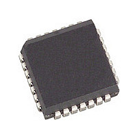
IC PROGRAM DELAY ECL 5V 28PLCC
Manufacturer
ON Semiconductor
Series
10Er
Type
Programmable Delay Chipr
Datasheet
1.MC100E195FNR2G.pdf
(11 pages)
Specifications of MC10E195FNG
Input
ECL
Output
ECL
Frequency - Max
1GHz
Voltage - Supply
4.2 V ~ 5.7 V
Operating Temperature
0°C ~ 85°C
Mounting Type
Surface Mount
Package / Case
28-PLCC
Frequency-max
1GHz
Lead Free Status / RoHS Status
Lead free / RoHS Compliant
Other names
MC10E195FNGOS
Available stocks
Company
Part Number
Manufacturer
Quantity
Price
Company:

Part Number:
MC10E195FNG
Manufacturer:
ON Semiconductor
Quantity:
10 000


V
V
LEN
SET MAX
SET MIN
D1
D0
EE
BB
IN
IN
* delays are 25% or 50% longer than
*
standard (standard ≈ 80 ps)
LEN
connected to Power Supply to guarantee proper operation.
LOGIC DIAGRAM AND PINOUT ASSIGNMENT
EN
Warning: All V
IN
IN
V
*All V
26
27
28
BB
1
2
3
4
V
EE
CC
* 1.25
D2
25
NC
Figure 1. Pinout: 28-Lead PLCC
5
and V
1
1
NC
D3
24
6
CC
CCO
1
0
, V
* 1.5
EN
D4
23
CCO
pins are tied together on the die.
7
MC100E195
(Top View)
MC10E195
, and V
D5
22
D0
1
8
0
EE
D6
21
9
1
D1
pins must be externally
1
0
D7
10
20
Figure 2. Logic Diagram − Simplified
D2
1
NC
19
11
7 BIT LATCH
1
18
17
16
15
14
13
12
1
D3
0
http://onsemi.com
NC
NC
V
V
Q
Q
V
CC
CCO
CCO
4 GATES
D4
2
D5
1
0
Table 1. PIN DESCRIPTION
Table 2. TRUTH TABLE
IN/IN
EN
D[0:7]
Q/Q
LEN
SET MIN
SET MAX
CASCADE, CASCADE
V
V
V
NC
BB
CC
EE
SETMAX
SETMAX
SETMIN
SETMIN
, V
LEN
LEN
EN.
EN
D6
8 GATES
CCO
PIN
LEN
LATCH
1
0
D7
D
Q
16 GATES
H
H
H
H
L
L
L
L
ECL Signal Input
ECL Input Enable
ECL MUX Select Inputs
ECL Signal Output
ECL Latch Enable
ECL Min Delay Set
ECL Max Delay Set
ECL Cascade Signal
Reference Voltage Output
Positive Supply
Negative Supply
No Connect
1
0
Pass Through D[0:10]
CASCADE
FUNCTION
Max Delay Path
Min Delay Path
1
Latch D[0:10]
Normal Mode
Normal Mode
Q Logic Low
1
0
Q = IN
Q
Q
CASCADE
CASCADE
Related parts for MC10E195FNG
Image
Part Number
Description
Manufacturer
Datasheet
Request
R

Part Number:
Description:
CONTACTOR, 1NO, 110VAC, 10A, DIN RAIL
Manufacturer:
IMO PRECISION CONTROLS
Datasheet:
Part Number:
Description:
CONTACTOR, 1NO, 230VAC, 10A, DIN RAIL
Manufacturer:
IMO PRECISION CONTROLS
Datasheet:
Part Number:
Description:
CONTACTOR, 1NO, 24VAC, 10A, DIN RAIL
Manufacturer:
IMO PRECISION CONTROLS
Datasheet:

Part Number:
Description:
5VDual TTL to Differential PECL Translator
Manufacturer:
ON Semiconductor
Datasheet:

Part Number:
Description:
Led Led Display Dot Matrix 5 X 7
Manufacturer:
Fema Electronics
Datasheet:
Part Number:
Description:
Led Led Display Dot Matrix 5 X 7
Manufacturer:
Fema Electronics
Datasheet:
Part Number:
Description:
ON Semiconductor [VOLTAGE REGULATOR]
Manufacturer:
ON Semiconductor
Datasheet:
Part Number:
Description:
357-036-542-201 CARDEDGE 36POS DL .156 BLK LOPRO
Manufacturer:
ON Semiconductor
Datasheet:
Part Number:
Description:
357-036-542-201 CARDEDGE 36POS DL .156 BLK LOPRO
Manufacturer:
ON Semiconductor
Datasheet:
Part Number:
Description:
357-036-542-201 CARDEDGE 36POS DL .156 BLK LOPRO
Manufacturer:
ON Semiconductor
Datasheet:
Part Number:
Description:
357-036-542-201 CARDEDGE 36POS DL .156 BLK LOPRO
Manufacturer:
ON Semiconductor
Datasheet:
Part Number:
Description:
357-036-542-201 CARDEDGE 36POS DL .156 BLK LOPRO
Manufacturer:
ON Semiconductor
Datasheet:
Part Number:
Description:
357-036-542-201 CARDEDGE 36POS DL .156 BLK LOPRO
Manufacturer:
ON Semiconductor
Datasheet:
Part Number:
Description:
357-036-542-201 CARDEDGE 36POS DL .156 BLK LOPRO
Manufacturer:
ON Semiconductor
Datasheet:
Part Number:
Description:
357-036-542-201 CARDEDGE 36POS DL .156 BLK LOPRO
Manufacturer:
ON Semiconductor
Datasheet: