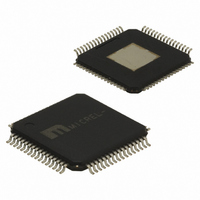
SY87721LHI Micrel Inc, SY87721LHI Datasheet - Page 5

SY87721LHI
Manufacturer Part Number
SY87721LHI
Description
IC CLOCK/DATA RECOVERY 64-TQFP
Manufacturer
Micrel Inc
Type
Clock and Data Recovery (CDR)r
Datasheet
1.SY87721LHY.pdf
(16 pages)
Specifications of SY87721LHI
Input
Differential
Output
Differential
Frequency - Max
340MHz
Voltage - Supply
3.15 V ~ 3.45 V
Operating Temperature
-40°C ~ 85°C
Mounting Type
Surface Mount
Package / Case
64-TQFP Exposed Pad, 64-eTQFP, 64-HTQFP, 64-VQFP
Frequency-max
340MHz
Lead Free Status / RoHS Status
Contains lead / RoHS non-compliant
Available stocks
Company
Part Number
Manufacturer
Quantity
Price
Micrel, Inc.
INPUTS
BRDMX [BRD Mux] – PECL Input
output. When logic HIGH, BRD is a direct copy of what
appears at RDOUTC . When logic low, BRD is a copy of
what appears at RDIN . Unlike RDOUTC , BRD conveys
valid data even when ENPECL is logic LOW. Please refer
to Table 1.
RDIN [Serial Data Input] – Differential PECL Input
stream. An internal receive PLL recovers the embedded
clock (RCLK) and data (RDOUT) information. The incoming
data rate can be within one of ten frequency ranges, or can
be one of five specific frequencies, depending on the state
of the FREQSEL and VCOSEL pins. The RDIN– pin has an
internal 75K resistor tied to V
REFCLK [Reference Clock] – Differential PECL Input
frequency synthesizer and the “training” frequency for the
receiver PLL to keep it centered in the absence of data
coming in on the RDIN input. The input frequency to
REFCLK is limited to 340MHz or less, depending on the
setting on the DIVSEL signals. The REFCLK– pin has an
internal 75K
CD [Carrier Detect] – PECL Input
PLL and can be driven by the carrier detect output of optical
modules or from external transition detection circuitry. When
this input is HIGH, the input data stream (RDIN) is recovered
normally by the Receive PLL. When this input is LOW, the
data on the RDOUT output will be internally forced to a
constant LOW, the Link Fault Indicator output LFIN forced
LOW, and the clock recovery PLL forced to lock onto the
synthesized clock frequency generated from REFCLK.
VCOSEL1, VCOSEL2 [VCO Select] – TTL Inputs
either one of three PLLs, or a SONET/SDH specific PLL.
Only the selected PLL is enabled. All other PLLs are
disabled. Refer to Table 3 for more details.
FREQSEL1, ..., FREQSEL3 [Frequency Select] – TTL Inputs
Refer to Table 3 for more details.
M9999-012508
hbwhelp@micrel.com or (408) 955-1690
PIN NAMES
This signal indicates what data appears at the BRD
This differential input accepts the receive serial data
This input is used as the reference for the internal
This input controls the recovery function of the Receive
These inputs select the output clock frequency range via
These inputs select the post divide ratio of the VCO.
BRDMX (Input)
0
1
resistor tied to V
Table 1. BRDMX Truth Table
CC
CC
.
.
BRD (Output)
RDOUTC
RDIN
5
DIVSEL1, ..., DIVSEL3 [Divider Select] – TTL Inputs
frequency (RCLK/TCLK) and the REFCLK input frequency
as shown in Table 4. Please note that the divide by 32
selection, “011”, is only available for use when FREQSEL
are set to “000.”
Note:
1. Some combinations of FREQSEL and DIVSEL result in undefined behavior.
CLKSEL [Clock Select] – TTL Input
the receiver PLL (CLKSEL = HIGH) or the clock of the
frequency synthesizer (CLKSEL = LOW) to the TCLK
outputs. Do not use for skew matching.
ENPECL [Enable ECL] – TTL Input
differential PECL outputs TCLKE , RDOUTE , and RCLKE .
It also disables the CML outputs, by setting TCLKC+,
RDOUTC+, and RCLKC+ logic HIGH and setting TCLKC–,
RDOUTC–, and RCLKC– logic LOW.
differential CML outputs TCLKC , RDOUTC , and RCLKC .
It also disables the PECL outputs by setting TCLKE+,
RDOUTE+, and RCLKE+ logic HIGH and setting TCLKE–,
RDOUTE– and RCLKE– logic LOW.
ALRSEL [Auto Lock Range Select] – TTL Input
frequency difference hysteresis at which ‘in-lock’ and ‘out of
lock’ conditions are declared. Please refer to the “AC
Characteristics” for more details.
These inputs select the ratio between the output clock
Refer to Table 3 for more details.
This input is used to select either the recovered clock of
This input, when HIGH (ENPECL = 1), enables the
When set LOW (ENPECL = 0), this signal enables the
This pin defines the frequency difference, and the
DIVSEL1
Table 2
0
0
0
0
1
1
1
1
(1)
. Reference Clock Multiplier Truth Table
DIVSEL2
0
0
1
1
0
0
1
1
DIVSEL3
0
1
0
1
0
1
0
1
Multiplier
REFCLK
SY87721L
32
10
16
20
1
2
4
8


