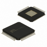
SY87721LHG Micrel Inc, SY87721LHG Datasheet

SY87721LHG
Specifications of SY87721LHG
Available stocks
Related parts for SY87721LHG
SY87721LHG Summary of contents
Page 1
Micrel, Inc. FEATURES Recovers any data and clock from 28Mbps to 2.7Gbps • OC-1, OC-3, OC-12, OC-48, ATM • Gigabit Ethernet, Fast Ethernet • Fibre Channel, 2x Fibre Channel • P1394, Infiniband • SMPTE-259, SMPTE-292 • Proprietary optical transport Integrated ...
Page 2
Micrel, Inc. PACKAGE/ORDERING INFORMATION VCOSEL1 1 48 PLLRN PLLRN— PLLRW PLLRW— ...
Page 3
Micrel, Inc. SYSTEM BLOCK DIAGRAM FIBER PIN DIODE TIA 27MHz SY889x2 FIBER LASER LASER DIODE DIODE DRIVER OC-48 EYE DIAGRAM M9999-012508 hbwhelp@micrel.com or (408) 955-1690 SY889x3 SY87721L ® AnyRate POST AMP CDR SY87729L CMU REF_CLK AnyClock™ Fractional Synthesizer SEL Time ...
Page 4
Micrel, Inc. FUNCTIONAL BLOCK DIAGRAM RDIN+ Phase RDIN— Detector/ Data Recovery Phase/ Frequency Detector CD REFCLK+ Phase/ REFCLK— Frequency Detector Divide 10, 16, 20, 32 M9999-012508 hbwhelp@micrel.com or (408) 955-1690 Charge VCO Pump N/W1/W2/W3 N/W ...
Page 5
Micrel, Inc. PIN NAMES INPUTS BRDMX [BRD Mux] – PECL Input This signal indicates what data appears at the BRD output. When logic HIGH, BRD is a direct copy of what appears at RDOUTC . When logic low, BRD is ...
Page 6
Micrel, Inc. OUTPUTS BRD [Buffered Recovered Data] – Differential CML Output The signal is either a buffered RDIN depending on the state of the BRDMX input. This allows a user to selectively bypass the CDR or not, as warranted by ...
Page 7
Micrel, Inc. DESCRIPTION General The SY87721L is a complete clock and data recovery circuit, capable of handling NRZ data rates from 28MHz through to 2.7GHz. A reference PLL is used as a frequency synthesizer, both to multiply a reference clock ...
Page 8
Micrel, Inc. LOOP FILTER COMPONENTS R PLLSN+ or PLLSW+ Figure 1. Narrow Band and Wide Band Synthesizer Loop Filter R PLLRN+ or PLLRW+ Figure 2. Narrow Band and Wide Band CDR Loop Filter PLL R PLLSN+, PLLSN– 1.2k PLLRN+, PLLRN– ...
Page 9
Micrel, Inc. ABSOLUTE MAXIMUM RATINGS Symbol V Power Supply Voltage CC V Input Voltage IN I ECL Output Current OUT I CML Output Current CMLOUT Lead Temperature (soldering, 20 sec.) T Storage Temperature Range store T Operating Temperature Range A ...
Page 10
Micrel, Inc. TTL DC ELECTRICAL CHARACTERISTICS 3.3V 5%; GND = GNDA = 0V CCO CCA Symbol Parameter V Input HIGH Voltage IH V Input LOW Voltage IL I Input HIGH Current IH I ...
Page 11
Micrel, Inc. TIMING WAVEFORMS REFCLK– RDOUT RCLK CML V DIAGRAM OSW CML Pin (True or Complement) M9999-012508 hbwhelp@micrel.com or (408) 955-1690 t t CPWL CPWH ODC ODC V (Single-Ended Swing) OSW 11 SY87721L V ...
Page 12
Micrel, Inc. EVALUATION BOARD SCHEMATIC R48 VCC R47, 130 S1 VEE DIP-5 VEE VCC L3 VCCA R7 C9 C10 HEADER 6X2 JP1 ...
Page 13
Micrel, Inc. EVALUATION BOARD I/O TERMINATION SCHEMES TCLK RCLK OUTPUTS OUTPUTS C19 J14 RCLKC– TCLKC– C20 J13 TCLKC+ RCLKC C21 J12 TCLKE– RCLKE– R30, 330 V EE C22 J11 TCLKE+ RCLKE R31, ...
Page 14
Micrel, Inc. REFCLK INPUTS V CC R40, 68.5 C35 J15 REFCLK+:FORCE 1 2 R41, 185 C36 J16 REFCLK+: SENSE R42, 68.5 C37 J19 REFCLK–:FORCE 1 2 R43, 185 C38 J20 REFCLK–: SENSE ...
Page 15
Micrel, Inc. 64 LEAD EPAD-TQFP (DIE UP) (H64-1) +0.03 –0.03 +0.012 –0.012 Heat Dissipation PCB Thermal Consideration for 64-Pin EPAD-TQFP Package M9999-012508 hbwhelp@micrel.com or (408) 955-1690 +0.05 –0.05 +0.002 –0.002 +0.05 –0.05 +0.012 –0.012 +0.05 –0.05 +0.002 –0.002 CompSide Island ...
Page 16
Micrel, Inc. Layout and General Suggestions 1. Establish controlled impedance stripline, microstrip, or co-planar construction techniques. 2. Signal paths should have, approximately, the same width as the device pads. 3. All differential paths are critical timing paths, where skew should ...


