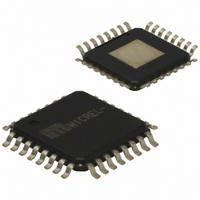
SY87701VSC Micrel Inc, SY87701VSC Datasheet - Page 3

SY87701VSC
Manufacturer Part Number
SY87701VSC
Description
IC CLOCK/DATA RECOVERY 32-TQFP
Manufacturer
Micrel Inc
Type
Clock and Data Recovery (CDR)r
Datasheet
1.SY87701VZH.pdf
(15 pages)
Specifications of SY87701VSC
Input
PECL, TTL
Output
PECL, TTL
Frequency - Max
1.25GHz
Voltage - Supply
3.15 V ~ 3.45 V, 4.75 V ~ 5.25 V
Operating Temperature
0°C ~ 85°C
Mounting Type
Surface Mount
Package / Case
32-TQFP Exposed Pad, 32-eTQFP, 32-HTQFP, 32-VQFP
Frequency-max
1.25GHz
Lead Free Status / RoHS Status
Contains lead / RoHS non-compliant
Available stocks
Company
Part Number
Manufacturer
Quantity
Price
Part Number:
SY87701VSC
Manufacturer:
MICREL/麦瑞
Quantity:
20 000
Micrel, Inc.
INPUTS
RDINP, RDINN [Serial Data Input] Differential PECL.
differential receive serial data stream. An internal receive
PLL recovers the embedded clock (RCLK) and data
(RDOUT) information. The incoming data rate can be within
one of eight frequency ranges depending on the state of
the FREQSEL pins. See “Frequency Selection” Table.
REFCLK [Reference Clock] TTL Input.
frequency synthesizer and the “training” frequency for the
receiver PLL to keep it centered in the absence of data
coming in on the RDIN inputs.
CD [Carrier Detect] PECL Input.
PLL and can be driven by the carrier detect output of optical
modules or from external transition detection circuitry. When
this input is HIGH the input data stream (RDIN) is recovered
normally by the Receive PLL. When this input is LOW the
data on the inputs RDIN will be internally forced to a constant
LOW, the data outputs RDOUT will remain LOW, the Link
Fault Indicator output LFIN forced LOW and the clock
recovery PLL forced to lock onto the clock frequency
generated from REFCLK.
FREQSEL1, ..., FREQSEL3 [Frequency Select] TTL
Inputs.
shown in the “Frequency Selection” Table.
DIVSEL1, DIVSEL2 [Divider Select] TTL Inputs.
frequency (RCLK/TCLK) and the REFCLK input frequency
as shown in the “Reference Frequency Selection” Table.
CLKSEL [Clock Select] TTL Input.
the receiver PLL (CLKSEL = HIGH) or the clock of the
frequency synthesizer (CLKSEL = LOW) to the TCLK
outputs.
M9999-073008
hbwhelp@micrel.com or (408) 955-1690
PIN DESCRIPTIONS
These built-in line receiver inputs are connected to the
This input is used as the reference for the internal
This input controls the recovery function of the Receive
These inputs select the output clock frequency range as
These inputs select the ratio between the output clock
This input is used to select either the recovered clock of
3
OUTPUTS
LFIN [Link Fault Indicator] TTL Output.
RDIN. Active HIGH signal is indicating when the internal
clock recovery PLL has locked onto the incoming data
stream. LFIN will go HIGH if CD is HIGH and RDIN is within
the frequency range of the Receive PLL (1000ppm). LFIN
is an asynchronous output.
RDOUTP, RDOUTN [Receive Data Output] Differential
PECL.
represent the recovered data from the input data stream
(RDIN). This recovered data is sampled on the rising edge
of RCLK.
RCLKP, RCLKN [Clock Output] Differential PECL.
represent the recovered clock used to sample the recovered
data (RDOUT).
TCLKP, TCLKN [Clock Output] Differential PECL.
represent either the recovered clock (CLKSEL = HIGH) used
to sample the recovered data (RDOUT) or the transmit clock
of the frequency synthesizer (CLKSEL = LOW).
PLLSP, PLLSN [Clock Synthesis PLL Loop Filter]
PLLRP, PLLRN [Clock Recovery PLL Loop Filter]
POWER & GROUND
V
V
V
GND
N/C
Note 1.
CC
CCA
CCO
This output indicates the status of the input data stream
These ECL 100K outputs (+3.3V or +5V referenced)
These ECL 100K outputs (+3.3V or +5V referenced)
These ECL 100K outputs (+3.3V or +5V referenced)
External loop filter pins for the clock synthesis PLL.
External loop filter pins for the receiver PLL.
V
CC
Supply Voltage
Analog Supply Voltage
Output Supply Voltage
Ground
No Connect
, V
CCA
, V
CCO
must be the same value.
(Note 1)
(Note 1)
(Note 1)
SY87701V


