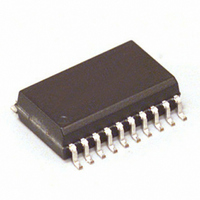
MC88LV926DWR2 Freescale Semiconductor, MC88LV926DWR2 Datasheet - Page 3

MC88LV926DWR2
Manufacturer Part Number
MC88LV926DWR2
Description
IC DRIVER CLK PLL 66MHZ 20-SOIC
Manufacturer
Freescale Semiconductor
Type
PLL Clock Driverr
Datasheet
1.MC88LV926DWR2.pdf
(12 pages)
Specifications of MC88LV926DWR2
Input
CMOS, TTL
Output
CMOS
Frequency - Max
66MHz
Voltage - Supply
3 V ~ 3.6 V
Operating Temperature
0°C ~ 70°C
Mounting Type
Surface Mount
Package / Case
20-SOIC (7.5mm Width)
Frequency-max
66MHz
Lead Free Status / RoHS Status
Contains lead / RoHS non-compliant
Other names
MC88LV926DWR2TR
Available stocks
Company
Part Number
Manufacturer
Quantity
Price
MAXIMUM RATINGS*
* Maximum Ratings are those values beyond which damage to the device may occur. Functional operation should be restricted to the
RECOMMENDED OPERATING CONDITIONS
DC CHARACTERISTICS (T A = 0 C to 70 C; V CC = 3.3V
1. I OL is +12mA for the RST_OUT output.
2. The PLL_EN input pin is not guaranteed to meet this specification.
3. Maximum test duration 2.0ms, one output loaded at a time.
4. The MC88LV926 can also be operated from a 5.0V supply. V OH output levels will vary 1:1 with V CC , input levels and current specs will be
TIMING SOLUTIONS
V CC , AV CC
V in
V out
I in
I out
I CC
T stg
V CC
V in
V out
T A
ESD
V IH
V IL
V OH
V OL
I IN
I CCT
I OLD
I OHD
I CC
Recommended Operating Conditions.
Symbol
unchanged, except V IH ; when V CC > 4.0 volts, V IH minimum level is 2.7 volts.
Symbol
Symbol
Minimum High Level Input Voltage
Minimum Low Level Input Voltage
Minimum High Level Output Voltage
Minimum Low Level Output Voltage
Maximum Input Leakage Current
Maximum I CC /Input
Minimum Dynamic 3 Output Current
Maximum Quiescent Supply Current
DC Supply Voltage Referenced to GND
DC Input Voltage (Referenced to GND)
DC Output Voltage (Referenced to GND)
DC Input Current, Per Pin
DC Output Sink/Source Current, Per Pin
DC V CC or GND Current Per Output Pin
Storage Temperature
Supply Voltage
DC Input Voltage
DC Output Voltage
Ambient Operating Temperature
Static Discharge Voltage
Parameter
4
Parameter
Parameter
V CC
3.0
3.3
3.0
3.3
3.0
3.3
3.0
3.3
3.3
3.3
3.3
3.3
3.3
0.3V) 4
3
Guaranteed Limits
2.0 2
0.55
0.55
–50
750
2.0
2.0
0.8
0.8
2.2
2.5
50
1.0
Unit
mA
mA
mA
V
V
V
V
A
A
–0.5 to V CC +0.5
–0.5 to V CC +0.5
–65 to +150
–0.5 to 7.0
0 to V CC
0 to V CC
3.3 0.3
Limits
Limits
0 to 70
> 1500
V OUT = 0.1V or
V CC – 0.1V
V OUT = 0.1V or
V CC – 0.1V
V IN = V IH or V IL
I OH
V IN = V IH or V IL
I OH
V I = V CC , GND
V I = V CC – 2.1V
V OLD = 1.25V Max
V OHD = 2.35 Min
V I = V CC , GND
20
50
50
Condition
MC88LV926
–24mA
–24mA
+24mA 1
+24mA
MOTOROLA
Unit
Unit
mA
mA
mA
V
V
V
V
V
V
V
C
C


