MIC74BQS Micrel Inc, MIC74BQS Datasheet - Page 2
MIC74BQS
Manufacturer Part Number
MIC74BQS
Description
IC I/O EXPANDER I2C 8B 16QSOP
Manufacturer
Micrel Inc
Series
-r
Datasheet
1.MIC74YQS.pdf
(18 pages)
Specifications of MIC74BQS
Interface
I²C, SMBus
Number Of I /o
8
Interrupt Output
Yes
Frequency - Clock
-
Voltage - Supply
2.7 V ~ 3.6 V
Operating Temperature
-40°C ~ 85°C
Mounting Type
Surface Mount
Package / Case
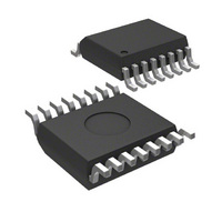
16-SSOP (0.154", 3.90mm Width)
Includes
-
Lead Free Status / Rohs Status
Contains lead / RoHS non-compliant


Pin Configuration
Pin Description
Micrel, Inc.
October 2006
Pin Number
9 – 12
1 – 3
4 – 7
13
14
15
16
8
(/SHDN, /FS0 – FS2)
Pin Name
A0 – A2
P0 – P3
P4 – P7
/ALERT
DATA
GND
VDD
CLK
Pin Function
Address (Input): Slave address selection inputs; sets the three least significant bits of the
MIC74’s slave address.
Parallel I/O (Input/Output): General-purpose I/O pin. Direction and output type are user
programmable.
Ground
Parallel I/O (Input/output): P4–P7 are general-purpose I/O pins. Direction and output type
are user programmable.
Shutdown (Output): When the FAN bit is set, pin 9 becomes SHDN.
Fan Speed (Output): When the FAN bit is set, pins 10 through 12 become /FS0–/FS2
respectively, controlled by the FAN_SPEED register.
Interrupt (Output): Active-low, open-drain output signals input-change-interrupts to the host
on this pin. Signal is cleared when the bus master (host) polls the ARA (alert response
address = 0001 100) or reads status.
Serial Bus Clock (Input): The host provides the serial bit clock in this input.
Serial Data (Input/Output): Serial data input and open-drain serial data output.
Power Supply (Input).
GND
A0
A1
A2
P0
P1
P2
P3
1
2
3
4
5
6
7
8
16-Pin QSOP (QS)
2
16 VDD
15
14
13
12
11
10
9
DATA
CLK
/ALERT
P7 (/FS2)
P6 (/FS1)
P5 (/FS0)
P4 (/SHDN0)
M9999-101006
MIC74
Related parts for MIC74BQS
Image
Part Number
Description
Manufacturer
Datasheet
Request
R

Part Number:
Description:
Manufacturer:
Micrel Inc
Datasheet:
Part Number:
Description:
Manufacturer:
Micrel Inc
Datasheet:
Part Number:
Description:
Manufacturer:
Micrel Inc
Datasheet:
Part Number:
Description:
Manufacturer:
Micrel Inc
Datasheet:
Part Number:
Description:
Manufacturer:
Micrel Inc
Datasheet:
Part Number:
Description:
Manufacturer:
Micrel Inc
Datasheet:
Part Number:
Description:
Manufacturer:
Micrel Inc
Datasheet:
Part Number:
Description:
Manufacturer:
Micrel Inc
Datasheet:
Part Number:
Description:
Manufacturer:
Micrel Inc
Datasheet:
Part Number:
Description:
Manufacturer:
Micrel Inc
Datasheet:
Part Number:
Description:
Manufacturer:
Micrel Inc
Datasheet:
Part Number:
Description:
Manufacturer:
Micrel Inc
Datasheet:
Part Number:
Description:
Manufacturer:
Micrel Inc
Datasheet:
Part Number:
Description:
Manufacturer:
Micrel Inc
Datasheet: