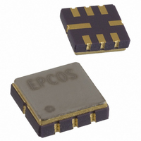
B39311B3577U310 EPCOS Inc, B39311B3577U310 Datasheet - Page 4
B39311B3577U310
Manufacturer Part Number
B39311B3577U310
Description
FILTER SAW 311.06MHZ REMOTE SMD
Manufacturer
EPCOS Inc
Datasheet
1.B39311B3577U310.pdf
(6 pages)
Specifications of B39311B3577U310
Insertion Loss
2dB
Frequency
311.06MHz Center
Filter Type
Bandpass
Applications
Remote Control
Package / Case
0.197" L x 0.197" W x 0.053" H (5.00mm x 5.00mm x 1.35mm)
Mounting Type
Surface Mount
Saw Filter Type
Low-Loss Filter
Center Frequency
311.06MHz
Pass Band Ripple (db)
3dB
Termination Impedance
50Ohm
Package Type
QCC8C
Case Height
1.35mm
Case Length
5mm
Case Depth
5mm
Mounting
Surface Mount
Pin Count
8
Operating Temp Range
-45C to 120C
Termination Style
SMD/SMT
Operating Temperature Range
- 45 C to + 120 C
Lead Free Status / RoHS Status
Lead free / RoHS Compliant
Bandwidth
-
Lead Free Status / Rohs Status
Details
Other names
495-2326-2
B39311B3577U310
B39311B3577U310


Data Sheet
Matching network to 50
SAW Components
Low-loss Filter
Minimising the crosstalk
For a good ultimate rejection a low crosstalk is necessary. Low crosstalk can be realised with
a good RF layout. The major crosstalk mechanism is caused by the “ground-loop” problem.
Grounding loops are created if input-and output transducer GND are connected on the top-side
of the PCB and fed to the system grounding plane by a common via hole. To avoid the common
ground path, the ground pin of the input- and output transducer are fed to the system ground
plane (bottom PCB plane) by their own via hole. The transducers’ grounding pins should be
isolated from the upper grounding plane.
A common GND inductivity of 0.5nH degrades the ultimate rejection (crosstalk) by 20dB.
The optimised PCB layout, including matching network for transformation to 50 Ohm, is shown
here. In this PCB layout the grounding loops are minimised to realise good ultimate rejection.
Optimised PCB layout for SAW filters in QCC8C package, pinning 2,5 (top side, scale 1:1)
The bottom side is a copper plane (system ground area). The input and output grounding pins
are isolated and connected to the common ground by separated via holes.
For good contact of the upper grounding area with the lower side it is necessary to place
enough via holes.
(element values depend on pcb layout and equivalent circuit)
4
Sep 09, 2005
L
L
s1
s2
= 56 nH
= 56 nH
311,06 MHz
B3577
Related parts for B39311B3577U310
Image
Part Number
Description
Manufacturer
Datasheet
Request
R

Part Number:
Description:
Manufacturer:
EPCOS Inc
Datasheet:

Part Number:
Description:
314,875 / 315,125 Mhz Resonator
Manufacturer:
EPCOS AG
Datasheet:
Part Number:
Description:
Saw Resonator
Manufacturer:
EPCOS AG
Datasheet:
Part Number:
Description:
Saw Resonator
Manufacturer:
EPCOS AG
Datasheet:
Part Number:
Description:
One Port Resonators
Manufacturer:
EPCOS AG
Datasheet:
Part Number:
Description:
Saw Components
Manufacturer:
EPCOS AG
Datasheet:
Part Number:
Description:
Saw Components
Manufacturer:
EPCOS AG
Datasheet:
Part Number:
Description:
SAW Components Low-loss Filter 311,06 MHz
Manufacturer:
EPCOS [EPCOS]
Datasheet:
Part Number:
Description:
SAW Components Low-Loss Filter 313,85 MHz
Manufacturer:
EPCOS [EPCOS]
Datasheet:
Part Number:
Description:
SAW Components Low-loss Filter 313,85 MHz
Manufacturer:
EPCOS [EPCOS]
Datasheet:
Part Number:
Description:
SAW Components Low-loss Filter 314,85 MHz
Manufacturer:
EPCOS [EPCOS]
Datasheet:

Part Number:
Description:
RESONATOR SAW CER 310MHZ SMD
Manufacturer:
EPCOS Inc
Datasheet:

Part Number:
Description:
R 771 RESONATOR
Manufacturer:
EPCOS Inc
Datasheet:
