SST112-T1-E3 Vishay, SST112-T1-E3 Datasheet
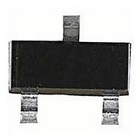
N CHANNEL JFET, -55V, SOT-23

SST112-T1-E3

Manufacturer Part Number
SST112-T1-E3
Description
N CHANNEL JFET, -55V, SOT-23
Manufacturer
Vishay
Datasheets

Specifications of SST112-T1-E3

Channel Type
N
Configuration
Single
Operating Temperature (min)
-55C
Operating Temperature (max)
150C
Operating Temperature Classification
Military
Mounting
Surface Mount
Pin Count
3
Breakdown Voltage Vbr
-55V
Gate-source Cutoff Voltage Vgs(off) Max
-5V
Power Dissipation Pd
350mW
Operating Temperature Range
-55°C To +150°C
No. Of Pins
3
Peak Reflow Compatible (260 C)
Yes
Leaded Process Compatible
Yes
Rohs Compliant
Yes
Lead Free Status / RoHS Status
Compliant

Available stocks

Company
Part Number
Manufacturer
Quantity
Price
Part Number:
SST112-T1-E3
Manufacturer:
VISHAY/威世
Quantity:
20 000
The J/SST111 series consists of all-purpose analog switches
designed to support a wide range of applications.
J/SST113 are useful in a high-gain amplifier mode.
The J series, TO-226AA (TO-92) plastic package, provides
low cost, while the SST series, TO236 (SOT-23) package,
provides surface-mount capability. Both the J and SST series
are available in tape-and-reel for automated assembly (see
Packaging Information).
Gate-Drain, Gate-Source Voltage
Gate Current
Lead Temperature (
Storage Temperature
Operating Junction Temperature
For applications information see AN105.
Document Number: 70232
S-04028—Rev. E, 04-Jun-01
D Low On-Resistance: 111 < 30 W
D Fast Switching—t
D Low Leakage: 5 pA
D Low Capacitance: 3 pF
D Low Insertion Loss
Part Number
J/SST111
J/SST112
J/SST113
. . . . . . . . . . . . . . . . . . . . . . . . . . . . . . . . . . . . . . . . . . . . . . . . .
1
/
16
. . . . . . . . . . . . . . . . . . . . . . . . . . . . . . . . . . .
” from case for 10 seconds)
G
V
D
S
TO-226AA (TO-92)
–3 to –10
GS(off)
–1 to –5
ON
v–3
: 4 ns
Top View
. . . . . . . . . . . . . . . . . . . . . . . . . .
(V)
. . . . . . . . . . . . . . . . . . . . . . . . . . . . . . .
J111
J112
J113
1
2
3
r
DS(on)
100
Max (W)
30
50
. . . . . . . . . . . . . .
D Low Error Voltage
D High-Speed Analog Circuit Performance
D Negligible “Off-Error,” Excellent Accuracy
D Good Frequency Response, Low Glitches
D Eliminates Additional Buffering
N-Channel JFETs
–55 to 150_C
–55 to 150_C
I
D(off)
300 _C
50 mA
–35 V
Typ (pA)
The
5
5
5
For similar products in TO-206AA(TO-18) packaging, see the
2N/PN/SST4391
2N5564/5565/5566 (duals) data sheets.
Power Dissipation
(TO-236)
(TO-226AA)
Notes
a.
t
ON
Derate 2.8 mW/_C above 25_C
Typ (ns)
. . . . . . . . . . . . . . . . . . . . . . . . . . . . . . . . . . . . . . . . . . . . . . . . . .
4
4
4
. . . . . . . . . . . . . . . . . . . . . . . . . . . . . . . . . . . . . . . . . . . . . . .
a
D
S
series,
*Marking Code for TO-236
1
2
TO-236 (SOT-23)
SST111 (C1)*
SST112 (C2)*
SST113 (C3)*
Top View
2N4856A/4857A/4858A,
J/SST111 Series
D Analog Switches
D Choppers
D Sample-and-Hold
D Normally “On” Switches
D Current Limiters
Vishay Siliconix
J112 SST112
J113 SST113
J111 SST111
3
G
www.vishay.com
350 mW
360 mW
7-1
and

Related parts for SST112-T1-E3

SST112-T1-E3 Summary of contents

Page 1

... Derate 2.8 mW/_C above 25_C J/SST111 Series Vishay Siliconix J111 SST111 J112 SST112 J113 SST113 D Analog Switches D Choppers D Sample-and-Hold D Normally “On” Switches D Current Limiters series, 2N4856A/4857A/4858A, TO-236 (SOT-23 Top View SST111 (C1)* SST112 (C2)* SST113 (C3)* *Marking Code for TO-236 www.vishay.com and 350 mW 360 mW 7-1 ...

Page 2

... V 0.005 125_C 0 0 kHz kHz MHz kHz GS(H) GS(H) See Switching Circuit 6 15 Limits J/SST112 J/SST113 Max Min Max Min Max Unit –35 – –10 –1 –5 – –1 –1 – 100 100 NCB Document Number: 70232 S-04028—Rev. E, 04-Jun-01 ...

Page 3

... Document Number: 70232 S-04028—Rev. E, 04-Jun-01 _ 200 = 0 160 I DSS 120 –8 – –2 V GS(off) –4 V – 105 125 ) –2 V GS(off J/SST111 Series Vishay Siliconix On-Resistance vs. Drain Current 100 –2 V GS(off –4 V – – Drain Current (mA) D Turn-On Switching 5 t approximately independent – ...

Page 4

... J/SST111 Series Vishay Siliconix Noise Voltage vs. Frequency 100 100 – Frequency (Hz) Gate Leakage Current 125_C 100 25_C 0 – Drain-Gate Voltage (V) DG Common-Gate Forward Admittance 100 25_C A – 0.1 100 200 f – Frequency (MHz) www.vishay.com 7-4 _ Forward Transconductance and Output Conductance 50 40 ...

Page 5

... Frequency (MHz) Output Characteristics –4 V GS(off 0.2 0.4 0.6 V – Drain-Source Voltage (V) DS J/SST111 J/SST112 V –12 V –7 V GS(L) 800 W 1600 D(on) *Non-inductive Rise Time < Rise Time 0.4 ns Fall Time < Input Resistance 10 MW Pulse Width 100 ns Input Capacitance 1.5 pF ...

Page 6

... Vishay disclaims any and all liability arising out of the use or application of any product described herein or of any information provided herein to the maximum extent permitted by law. The product specifications do not expand or otherwise modify Vishay’ ...

Related keywords