2N5339JANTX MICROSEMI, 2N5339JANTX Datasheet
2N5339JANTX
Specifications of 2N5339JANTX


Related parts for 2N5339JANTX


2N5339JANTX Summary of contents
Page 1
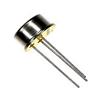
... Lake Street, Lawrence, MA 01841 1-800-446-1158 / (978) 620-2600 / Fax: (978) 689-0803 Website: http://www.microsemi.com NPN POWER SILICON SWITCHING TRANSISTOR DEVICES 2N5339 ABSOLUTE MAXIMUM RATINGS (T Parameters / Test Conditions Collector-Emitter Voltage Collector-Base Voltage Emitter-Base Voltage Base Current Collector Current @ T Total Power Dissipation @ Operating & Storage Junction Temperature Range ...
Page 2
... Lake Street, Lawrence, MA 01841 1-800-446-1158 / (978) 620-2600 / Fax: (978) 689-0803 Website: http://www.microsemi.com ELECTRICAL CHARACTERISTICS (T Parameters / Test Conditions (3) ON CHARACTERISTICS Forward-Current Transfer Ratio I = 0.5Adc 2.0Vdc 2.0Adc 2.0Vdc 5.0Adc 2.0Vdc C CE Collector-Emitter Saturation Voltage I = 2.0Adc 0.2Adc 5.0Adc 0.5Adc C B Base-Emitter Saturation Voltage ...
Page 3
... Lake Street, Lawrence, MA 01841 1-800-446-1158 / (978) 620-2600 / Fax: (978) 689-0803 Website: http://www.microsemi.com NOTES: 1. Dimensions are in inches. 2. Millimeters are given for general information only. 3. Symbol TL is measured from HD maximum. 4. Details of outline in this zone are optional. 5. Symbol CD shall not vary more than .010 (0.25 mm) in zone P. This zone is controlled for automatic handling. ...
Page 4
... Lake Street, Lawrence, MA 01841 1-800-446-1158 / (978) 620-2600 / Fax: (978) 689-0803 Website: http://www.microsemi.com NOTES: 1. Dimensions are in inches. 2. Millimeters are given for general information only accordance with ASME Y14.5M, diameters are equivalent to φx symbology. 4. Terminal 1 - collector, terminal 2 -base, terminal 3 - emitter. FIGURE 2. Physical dimensions and configuration (U3) (SMD 5) (TO-276AA) T4-LDS-0011 Rev ...