PALCE20V8-25JCT Cypress Semiconductor Corp, PALCE20V8-25JCT Datasheet
PALCE20V8-25JCT
Specifications of PALCE20V8-25JCT


Related parts for PALCE20V8-25JCT


PALCE20V8-25JCT Summary of contents
Page 1
... It is implemented with the familiar sum-of-product (AND-OR) logic structure and the programmable macrocell. The PALCE20V8 is executed in a 24-pin 300-mil molded DIP, a 300-mil cerdip, a 28-lead square ceramic leadless chip carrier, a 28-lead square plastic leaded chip carrier, and a 24-lead quarter size outline. The device provides inputs and 8 outputs ...
Page 2
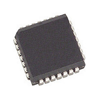
... GND Selection Guide t PD Generic Part Number Com’l/Ind PALCE20V8−5 5 PALCE20V8−7 7.5 PALCE20V8−10 10 PALCE20V8−15 15 PALCE20V8−25 25 PALCE20V8L−15 15 PALCE20V8L−25 25 Shaded areas contain preliminary information. Document #: 38-03026 Rev. *B USE ULTRA37000 FOR TM ALL NEW DESIGNS PLCC/LCC Top View ...
Page 3
... Power-Up Reset All registers in the PALCE20V8 power- logic LOW for predictable system initialization. For each register, the associated output pin will be HIGH due to active-LOW outputs. Configuration Table ...
Page 4
... Max Output Open MHz 15L, 25L ns (counter) 10, 15 15L, 25L ns Test Conditions MHz 2. MHz OUT Test Conditions Normal Programming Conditions PALCE20V8 [1] Ambient Temperature V CC ° ° 5V ± +75 C ° ° −40 5V ±10 +85 C ° ° −55 5V ±10 +125 C Min. ...
Page 5
... Min. Max. Min. Max. Min 7 max. OL internal (1 measured (see Note 7 above) minus t MAX MAX3 PALCE20V8 ≤ Military R R Measured Output Value 1 2 750Ω 1.5V 1.5V H ⎜ − 0. ⎜ 0.5V OL 20V8−15 20V8−25 Max. Min. Max. Min. Max. Unit ...
Page 6
... Min. Max. [ [8] 10 [8,10 62.5 62.5 [8,13 [8] 1 PALCE20V8 [3] 20V8−15 20V8−25 Max. Min. Max. Min. Max. Unit 45.5 37 MHz 62.5 41.6 MHz 50 40 MHz 20V8−15 20V8−25 Min. Max. Min. Max. Unit ...
Page 7
... INPUTS, I/O, REGISTERED FEEDBACK REGISTERED OUTPUTS COMBINATORIAL OUTPUTS Power-Up Reset Waveform 10% POWER SUPPLY VOLTAGE REGISTERED ACTIVE LOW OUTPUTS CLOCK Document #: 38-03026 Rev. *B USE ULTRA37000 FOR TM ALL NEW DESIGNS 90 MAX = 1 µ PALCE20V8 [11] [11 PXZ ER EA PZX [11] [11 PXZ ER EA PZX Page [+] Feedback ...
Page 8
... Functional Logic Diagram for PALCE20V8 PIN NUMBERS DIP (PLCC) PACKAGE 1 ( (3) 0 280 3 (4) 320 600 4 (5) 640 920 5 (6) 960 1240 6 (7) 1280 1560 7 (9) 1600 1880 8 (10) 1920 2200 9 (11) 2240 2520 10 (12) 11 (13) ELECTRONIC SIGNATURE ROW 2568 2569 . . . ...
Page 9
... PALCE20V8−15QI PALCE20V8−15DMB PALCE20V8−15LMB PALCE20V8−25JC PALCE20V8−25PC PALCE20V8−25QC 130 PALCE20V8−25JI PALCE20V8−25PI PALCE20V8−25QI PALCE20V8−25DMB PALCE20V8−25LMB Shaded areas contain preliminary information. Ordering Information for PALCE20V8L (mA) (ns) (ns) (ns) Ordering Code PALCE20V8L−15JC PALCE20V8L−15PC PALCE20V8L−15QC ...
Page 10
... Ordering Information for PALCE20V8L (mA) (ns) (ns) (ns) Ordering Code PALCE20V8L−25JI PALCE20V8L−25PI PALCE20V8L−25QI PALCE20V8L−25DMB PALCE20V8L−25LMB Document #: 38-03026 Rev. *B USE ULTRA37000 FOR TM ALL NEW DESIGNS (continued) Package Name J64 28-Lead Plastic Leaded Chip Carrier P13 24-Lead (300-Mil) Molded DIP ...
Page 11
... MILITARY SPECIFICATIONS Group Subgroup Testing DC Characteristics Parameter Switching Characteristics Parameter Package Diagrams Document #: 38-03026 Rev. *B USE ULTRA37000 FOR TM ALL NEW DESIGNS Subgroups Subgroups 24-Lead (300-Mil) CerDIP D14 MIL-STD-1835 D- 9 Config.A PALCE20V8 51-80031-** Page [+] Feedback ...
Page 12
... Package Diagrams (continued) Document #: 38-03026 Rev. *B USE ULTRA37000 FOR TM ALL NEW DESIGNS 28-Lead Plastic Leaded Chip Carrier J64 28-Square Leadless Chip Carrier L64 MIL-STD-1835 C-4 PALCE20V8 51-85001-*A 51-80051-** Page [+] Feedback ...
Page 13
... Semiconductor products in life-support systems application implies that the manufacturer assumes all risk of such use and in doing so indemnifies Cypress Semiconductor against all charges. USE ULTRA37000 FOR TM ALL NEW DESIGNS 24-Lead (300-Mil) PDIP P13 24-Lead Quarter Size Outline Q13 PALCE20V8 51-85013-*B 51-85055-B Page [+] Feedback ...
Page 14
... Document History Page Document Title: PALCE20V8 Flash-Erasable Reprogrammable CMOS PAL Document Number: 38-03026 REV. ECN NO. Issue Date ** 106371 07/11/01 *A 122231 12/28/02 *B 213375 See ECN Document #: 38-03026 Rev. *B USE ULTRA37000 FOR TM ALL NEW DESIGNS ® Orig. of Change Description of Change SZV Changed from Spec Number: 38-00367 to 38-03026 ...