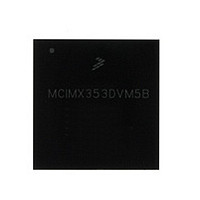
MCIMX353DVM5B Freescale, MCIMX353DVM5B Datasheet - Page 55

MCIMX353DVM5B
Manufacturer Part Number
MCIMX353DVM5B
Description
Manufacturer
Freescale
Datasheet
1.MCIMX353DVM5B.pdf
(148 pages)
Specifications of MCIMX353DVM5B
Operating Temperature (min)
-20C
Operating Temperature (max)
70C
Operating Temperature Classification
Commercial
Mounting
Surface Mount
Lead Free Status / RoHS Status
Compliant
Available stocks
Company
Part Number
Manufacturer
Quantity
Price
Company:
Part Number:
MCIMX353DVM5B
Manufacturer:
Freescale Semiconductor
Quantity:
10 000
Part Number:
MCIMX353DVM5B
Manufacturer:
FREESCALE
Quantity:
20 000
- Current page: 55 of 148
- Download datasheet (3Mb)
Freescale Semiconductor
SD21 DQS – DQ Skew (defines the Data valid window in read cycles related to DQS).
SD22 DQS DQ HOLD time from DQS
SD23 DQS output access time from SDCLK posedge
ID
DQS (input)
DQ (input)
SDCLK
SDCLK
Figure 36. Mobile DDR SDRAM DQ versus DQS and SDCLK Read Cycle Timing Diagram
SDRAM CLK and DQS-related parameters are measured from the 50%
point—that is, “high” is defined as 50% of signal value and “low” is defined
as 50% of signal value.
The timing parameters are similar to the ones used in SDRAM data sheets.
Table 41
the ESDCTL at the negative edge of SDCLK, and the parameters are
measured at maximum memory frequency.
SDRAM CLK and DQS-related parameters are measured from the 50%
point—that is, “high” is defined as 50% of signal value, and “low” is
defined as 50% of signal value.
The timing parameters are similar to the ones used in SDRAM data sheets.
Table 42
the ESDCTL at the negative edge of SDCLK, and the parameters are
measured at maximum memory frequency.
i.MX35 Applications Processors for Industrial and Consumer Products, Rev. 9
Table 42. Mobile DDR SDRAM Read Cycle Timing Parameters
indicates SDRAM requirements. All output signals are driven by
indicates SDRAM requirements. All output signals are driven by
SD23
SD21
Data
Parameter
SD22
Data
NOTE
NOTE
Data
Data
Data
Data
tDQSCK
Symbol
tDQSQ
tQH
Data
Min. Max. Unit
2.3
—
—
Data
0.85
6.7
—
ns
ns
ns
55
Related parts for MCIMX353DVM5B
Image
Part Number
Description
Manufacturer
Datasheet
Request
R
Part Number:
Description:
MCIMX-LVDS1
Manufacturer:
Freescale Semiconductor
Datasheet:

Part Number:
Description:
TOWER ELEVATOR BOARDS HARDWARE
Manufacturer:
Freescale Semiconductor
Datasheet:

Part Number:
Description:
TOWER SERIAL I/O HARDWARE
Manufacturer:
Freescale Semiconductor
Datasheet:

Part Number:
Description:
LCD MODULE FOR TWR SYSTEM
Manufacturer:
Freescale Semiconductor
Datasheet:

Part Number:
Description:
DAUGHTER LCD WVGA I.MX51
Manufacturer:
Freescale Semiconductor
Datasheet:

Part Number:
Description:
TOWER SYSTEM BOARD MPC5125
Manufacturer:
Freescale Semiconductor
Datasheet:

Part Number:
Description:
KIT EVALUATION I.MX51
Manufacturer:
Freescale Semiconductor
Datasheet:

Part Number:
Description:
KIT DEVELOPMENT WINCE IMX25
Manufacturer:
Freescale Semiconductor
Datasheet:

Part Number:
Description:
TOWER SYSTEM KIT MPC5125
Manufacturer:
Freescale Semiconductor
Datasheet:

Part Number:
Description:
TOWER SYSTEM BOARD K40X256
Manufacturer:
Freescale Semiconductor
Datasheet:

Part Number:
Description:
TOWER SYSTEM KIT K40X256
Manufacturer:
Freescale Semiconductor
Datasheet:

Part Number:
Description:
Microcontrollers (MCU) MX28 PLATFORM DEV KIT
Manufacturer:
Freescale Semiconductor
Datasheet:

Part Number:
Description:
MCU, MPU & DSP Development Tools IAR KickStart Kit for Kinetis K60
Manufacturer:
Freescale Semiconductor
Datasheet:

Part Number:
Description:
24BIT HDMI MX535/08
Manufacturer:
Freescale Semiconductor
Datasheet:
Part Number:
Description:
Manufacturer:
Freescale Semiconductor, Inc
Datasheet:


