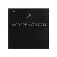
MC9328MX21CVM Freescale, MC9328MX21CVM Datasheet - Page 5

MC9328MX21CVM
Manufacturer Part Number
MC9328MX21CVM
Description
Manufacturer
Freescale
Datasheet
1.MC9328MX21CVM.pdf
(100 pages)
Specifications of MC9328MX21CVM
Operating Temperature (min)
-40C
Operating Temperature (max)
85C
Operating Temperature Classification
Industrial
Mounting
Surface Mount
Lead Free Status / RoHS Status
Compliant
Available stocks
Company
Part Number
Manufacturer
Quantity
Price
Company:
Part Number:
MC9328MX21CVM
Manufacturer:
Freescale Semiconductor
Quantity:
10 000
Company:
Part Number:
MC9328MX21CVMR2
Manufacturer:
Freescale Semiconductor
Quantity:
10 000
2
Table 2
Assignment and Package
manual.
The connections of the pins in
factory test signals that are not used in a normal application. Following is a list of these signals and how
they are to be terminated for proper operation of the i.MX21 processor:
Freescale Semiconductor
•
•
•
•
•
•
•
•
Signal Name
A [25:0]
D [31:0]
Memory Interface
— External Interface Module (EIM)
— SDRAM Controller (SDRAMC)
— NAND Flash Controller (NFC)
— PCMCIA/CF Interface
Standard System Resources
— Clock Generation Module (CGM) and Power Control Module
— Three General-Purpose 32-Bit Counters/Timers
— Watchdog Timer
— Real-Time Clock/Sampling Timer (RTC)
— Pulse-Width Modulator (PWM) Module
— Direct Memory Access Controller (DMAC)
— General-Purpose I/O (GPIO) Ports
— Debug Capability
Signal Descriptions
CLKMODE[1:0]: To ensure proper operation, leave these signals as no connects.
OSC26M_TEST: To ensure proper operation, leave this signal as no connect.
EXT_48M: To ensure proper operation, connect this signal to ground.
EXT_266M: To ensure proper operation, connect this signal to ground.
TEST_WB[2:0]: These signals are also multiplexed with GPIO PORT E as well as alternate
keypad signals. If not utilizing these signals for GPIO functionality or for their other multiplexed
function, then configure as GPIO input with pull up enabled, and leave as a no connect.
TEST_WB[4:3]: To ensure proper operation, leave these signals as no connects.
EB0
identifies and describes the i.MX21 signals. Pin assignment is provided in
Address bus signals
Data bus signals
MSB Byte Strobe—Active low external enable byte signal that controls D [31:24], shared with SDRAM
DQM0.
Information” and in the “Signal Multiplexing Scheme” table within the reference
Table 2
Table 2. i.MX21 Signal Descriptions
MC9328MX21 Technical Data, Rev. 3.4
depends solely upon the user application, however there are a few
External Bus/Chip Select (EIM)
Function/Notes
Section 4, “Pin
Signal Descriptions
5


