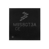
MC9S08GT32ACFDE Freescale, MC9S08GT32ACFDE Datasheet - Page 230

MC9S08GT32ACFDE
Manufacturer Part Number
MC9S08GT32ACFDE
Description
Manufacturer
Freescale
Datasheet
1.MC9S08GT32ACFDE.pdf
(302 pages)
Specifications of MC9S08GT32ACFDE
Cpu Family
HCS08
Device Core Size
8b
Frequency (max)
40MHz
Interface Type
I2C/SCI/SPI
Total Internal Ram Size
2KB
# I/os (max)
39
Number Of Timers - General Purpose
4
Operating Supply Voltage (typ)
2.5/3.3V
Operating Supply Voltage (max)
3.6V
Operating Supply Voltage (min)
1.8/2.08V
On-chip Adc
8-chx10-bit
Instruction Set Architecture
CISC
Operating Temp Range
-40C to 85C
Operating Temperature Classification
Industrial
Mounting
Surface Mount
Pin Count
48
Package Type
QFN EP
Program Memory Type
Flash
Program Memory Size
32KB
Lead Free Status / RoHS Status
Compliant
- Current page: 230 of 302
- Download datasheet (8Mb)
Analog-to-Digital Converter (S08ATDV3)
14.3.3
The analog input multiplexer selects one of the eight external analog input channels to generate an analog
sample. The analog input multiplexer includes negative stress protection circuitry which prevents
cross-talk between channels when the applied input potentials are within specification. Only analog input
signals within the potential range of V
conversions.
14.3.4
Figure 14-4
voltage in millivolts. The vertical axis the conversion result code. The ATD is specified with the following
figures of merit:
230
•
•
•
•
•
•
Number of bits (N) — The number of bits in the digitized output
Resolution (LSB) — The resolution of the ATD is the step size of the ideal transfer function. This
is also referred to as the ideal code width, or the difference between the transition voltages to a
given code and to the next code. This unit, known as 1LSB, is equal to
Inherent quantization error (E
straight-line transfer function into the quantized ideal transfer function with 2
± 1/2 LSB.
Differential non-linearity (DNL) — This is the difference between the current code width and the
ideal code width (1LSB). The current code width is the difference in the transition voltages to the
current code and to the next code. A negative DNL means the transfer function spends less time at
the current code than ideal; a positive DNL, more. The DNL cannot be less than –1.0; a DNL of
greater than 1.0 reduces the effective number of bits by 1.
Integral non-linearity (INL) — This is the difference between the transition voltage to the current
code and the transition to the corresponding code on the adjusted transfer curve. INL is a measure
of how straight the line is (how far it deviates from a straight line). The adjusted ideal transition
voltage is:
Zero scale error (E
and the ideal transition to that code. Normally, it is defined as the difference between the actual and
ideal transition to code 0x001, but in some cases the first transition may be to a higher code. The
ideal transition to any code is:
Adjusted Ideal Trans. V =
Analog Input Multiplexer
ATD Module Accuracy Definitions
illustrates an ideal ATD transfer function. The horizontal axis represents the ATD input
Ideal Transition V =
ZS
) — This is the difference between the transition voltage to the first valid code
1LSB = (V
Q
MC9S08GB60A Data Sheet, Rev. 2
(Current Code - 1/2)
REFL
) — This is the error caused by the division of the perfect ideal
(Current Code - 1/2)
to V
REFH
2
REFH
N
– V
2
REFL
N
(ATD reference potentials) will result in valid ATD
) / 2
* ((V
N
REFH
*(V
REFH
+ E
FS
– V
) - (V
REFL
REFL
)
Freescale Semiconductor
N
steps. This error is
+ E
ZS
))
Eqn. 14-5
Eqn. 14-6
Eqn. 14-7
Related parts for MC9S08GT32ACFDE
Image
Part Number
Description
Manufacturer
Datasheet
Request
R

Part Number:
Description:
TOWER ELEVATOR BOARDS HARDWARE
Manufacturer:
Freescale Semiconductor
Datasheet:

Part Number:
Description:
TOWER SERIAL I/O HARDWARE
Manufacturer:
Freescale Semiconductor
Datasheet:

Part Number:
Description:
LCD MODULE FOR TWR SYSTEM
Manufacturer:
Freescale Semiconductor
Datasheet:

Part Number:
Description:
DAUGHTER LCD WVGA I.MX51
Manufacturer:
Freescale Semiconductor
Datasheet:

Part Number:
Description:
TOWER SYSTEM BOARD MPC5125
Manufacturer:
Freescale Semiconductor
Datasheet:

Part Number:
Description:
KIT EVALUATION I.MX51
Manufacturer:
Freescale Semiconductor
Datasheet:

Part Number:
Description:
KIT DEVELOPMENT WINCE IMX25
Manufacturer:
Freescale Semiconductor
Datasheet:

Part Number:
Description:
TOWER SYSTEM KIT MPC5125
Manufacturer:
Freescale Semiconductor
Datasheet:

Part Number:
Description:
TOWER SYSTEM BOARD K40X256
Manufacturer:
Freescale Semiconductor
Datasheet:

Part Number:
Description:
TOWER SYSTEM KIT K40X256
Manufacturer:
Freescale Semiconductor
Datasheet:

Part Number:
Description:
Microcontrollers (MCU) MX28 PLATFORM DEV KIT
Manufacturer:
Freescale Semiconductor
Datasheet:

Part Number:
Description:
MCU, MPU & DSP Development Tools IAR KickStart Kit for Kinetis K60
Manufacturer:
Freescale Semiconductor
Datasheet:

Part Number:
Description:
24BIT HDMI MX535/08
Manufacturer:
Freescale Semiconductor
Datasheet:
Part Number:
Description:
Manufacturer:
Freescale Semiconductor, Inc
Datasheet:
Part Number:
Description:
Manufacturer:
Freescale Semiconductor, Inc
Datasheet:


