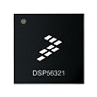
XC56309VF100A Freescale, XC56309VF100A Datasheet - Page 19

XC56309VF100A
Manufacturer Part Number
XC56309VF100A
Description
Manufacturer
Freescale
Datasheet
1.XC56309VF100A.pdf
(108 pages)
Specifications of XC56309VF100A
Device Core Size
24b
Format
Fixed Point
Clock Freq (max)
100MHz
Mips
100
Device Input Clock Speed
100MHz
Ram Size
102KB
Operating Supply Voltage (typ)
3.3V
Operating Supply Voltage (min)
3V
Operating Supply Voltage (max)
3.6V
Operating Temp Range
-40C to 100C
Operating Temperature Classification
Industrial
Mounting
Surface Mount
Pin Count
196
Package Type
MA-BGA
Lead Free Status / RoHS Status
Not Compliant
Available stocks
Company
Part Number
Manufacturer
Quantity
Price
Company:
Part Number:
XC56309VF100A
Manufacturer:
MOTOLOLA
Quantity:
437
Company:
Part Number:
XC56309VF100A
Manufacturer:
Freescale Semiconductor
Quantity:
10 000
Part Number:
XC56309VF100A
Manufacturer:
FREESCALE
Quantity:
20 000
Company:
Part Number:
XC56309VF100AR2
Manufacturer:
Freescale Semiconductor
Quantity:
10 000
1.11 Timers
The DSP56309 has three identical and independent timers. Each timer can use internal or external clocking and can
either interrupt the DSP56309 after a specified number of events (clocks) or signal an external device after
counting a specific number of internal events.
Freescale Semiconductor
TIO0
TIO1
TIO2
Notes:
Signal Name
1.
2.
3.
In the Stop state, the signal maintains the last state as follows:
• If the last state is input, the signal is an ignored input.
• If the last state is output, the signal is tri-stated.
The Wait processing state does not affect the signal state.
All inputs are 5 V tolerant.
Input or Output
Input or Output
Input or Output
Type
Ignored Input
Ignored Input
Ignored Input
State During
Reset
Table 1-15.
DSP56309 Technical Data, Rev. 7
1,2
Timer 0 Schmitt-Trigger Input/Output— When Timer 0 functions as an
external event counter or in measurement mode, TIO0 is used as input. When
Timer 0 functions in watchdog, timer, or pulse modulation mode, TIO0 is used
as output.
The default mode after reset is GPIO input. TIO0 can be changed to output or
configured as a timer I/O through the Timer 0 Control/Status Register (TCSR0).
Timer 1 Schmitt-Trigger Input/Output— When Timer 1 functions as an
external event counter or in measurement mode, TIO1 is used as input. When
Timer 1 functions in watchdog, timer, or pulse modulation mode, TIO1 is used
as output.
The default mode after reset is GPIO input. TIO1 can be changed to output or
configured as a timer I/O through the Timer 1 Control/Status Register (TCSR1).
Timer 2 Schmitt-Trigger Input/Output— When Timer 2 functions as an
external event counter or in measurement mode, TIO2 is used as input. When
Timer 2 functions in watchdog, timer, or pulse modulation mode, TIO2 is used
as output.
The default mode after reset is GPIO input. TIO2 can be changed to output or
configured as a timer I/O through the Timer 2 Control/Status Register (TCSR2).
Triple Timer Signals
Signal Description
Timers
1-15


