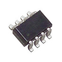
LTC2906ITS8#PBF Linear Technology, LTC2906ITS8#PBF Datasheet - Page 9

LTC2906ITS8#PBF
Manufacturer Part Number
LTC2906ITS8#PBF
Description
Manufacturer
Linear Technology
Datasheet
1.LTC2906ITS8PBF.pdf
(16 pages)
Specifications of LTC2906ITS8#PBF
Voltage Supervisor Type
Voltage Monitor
Number Of Voltage Supervisors
2
Monitored Supervisor Voltage
5/3.3/2.5/Adj
Package Type
TSOT-23
Operating Temperature Classification
Industrial
Operating Temp Range
-40C to 85C
Pin Count
8
Mounting
Surface Mount
Lead Free Status / RoHS Status
Compliant
Available stocks
Company
Part Number
Manufacturer
Quantity
Price
APPLICATIO S I FOR ATIO
In margining application, the three-state input pins can be
driven using a three-state buffer. Note however, the low
and high output of the three-state buffer has to satisfy the
V
Characteristics Table. Moreover, when the three-state
buffer is in the high impedance state, the maximum
leakage current allowed from the pin to either GND or V1
is 10 A.
Monitor Programming
Connecting S1 to either GND, or V1, or leaving it in open
state selects the LTC2906/LTC2907 V1 input voltage
threshold. Table 1 shows the three possible selections of
V1 nominal input voltage and their corresponding S1
connection.
The noninverting input on the V
to 0.5V when the TOL pin is set high (5% tolerance)
(Figure 1) and the high impedance inverting input directly
ties to the V
In a typical application, the V
on an external resistive divider between the positive volt-
age being monitored and ground. The following formula
obtains R1 resistor value for a particular value of R2 and
a desired trip voltage at 5% tolerance:
IL
R
and V
1
Table 1. Supply Selection Programming
Note: Open = open circuit or driven by a three-state buffer
in high impedance state with leakage current less than 10 A.
V
IH
Figure 1. Setting the Adjustable Trip Point
TRIP
ADJ
0 5
of the three-state pin listed in the Electrical
.
V
5 ( %)
V
ADJ
pin.
V
5.0
3.3
2.5
TRIP
V1
U
R1
1%
R2
1%
–
1 2
+
–
R
0.5V
U
LTC2906/LTC2907
–
+
ADJ
pin connects to a tap point
ADJ
W
OPEN
GND
S1
V1
comparator is set
29067 F01
U
R2 =100k is recommended. Once the resistor divider is
set in the 5% tolerance mode, there is no need to change
the divider for the other tolerance modes (7.5%, 10%)
because the internal reference at the noninverting input on
the V
point in 2.5% decrements.
Table 2 shows suggested 1% resistor values for various
adjustable applications.
Table 2. Suggested 1% Resistor Values for the V
Tolerance Programming
The three-state input pin TOL, programs the common
supply tolerance for both V1 and V
7.5% or 10%). The larger the tolerance the lower the trip
threshold. Table 3 shows the tolerances selection corre-
sponding to a particular connection at the TOL pin.
V
SUPPLY
ADJ
7.5
3.3
2.5
1.8
1.5
1.2
0.9
0.8
0.7
0.6
12
10
8
6
5
3
1
comparator is scaled accordingly, moving the trip
(V)
Table 3. Tolerance Programming
TOLERANCE
7.5%
10%
V
5%
TRIP
11.25
4.725
3.055
2.325
1.685
1.410
1.120
0.933
0.840
0.750
0.655
0.561
2.82
7.5
5.6
9.4
LTC2906/LTC2907
7
(V)
R1 (k )
ADJ
2150
1780
1400
1300
1020
86.6
68.1
49.9
30.9
12.1
845
464
511
365
237
182
124
OPEN
GND
TOL
V1
input voltages (5%,
ADJ
Inputs
R2 (k )
100
100
100
100
100
100
100
100
100
100
100
100
100
100
100
100
100
29067f
9


