AFBR732B Avago Technologies US Inc., AFBR732B Datasheet - Page 5
AFBR732B
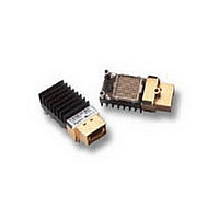
Manufacturer Part Number
AFBR732B
Description
Manufacturer
Avago Technologies US Inc.
Datasheet
1.AFBR732B.pdf
(22 pages)
Specifications of AFBR732B
Optical Fiber Type
TX/RX
Data Transfer Rate
2500MBd
Optical Rise Time
0.15ns
Optical Fall Time
0.15ns
Jitter
0.162ns
Operating Temperature Classification
Commercial
Peak Wavelength
850/860nm
Operating Supply Voltage (min)
3.135V
Operating Supply Voltage (typ)
3.3V
Operating Supply Voltage (max)
3.465V
Output Current
25mA
Operating Temp Range
0C to 80C
Mounting
Screw
Pin Count
100
Lead Free Status / RoHS Status
Compliant


Absolute Maximum Ratings
Notes:
1. Absolute Maximum Ratings are those values beyond which damage to the device may occur. See Reliability Data Sheet for specific reliability
2. Between Absolute Maximum Ratings and the Recommended Operating Conditions functional performance is not intended, device reliability
3. This is the maximum voltage that can be applied across the Transmitter Differential Data Inputs without damaging the input circuit.
4. Case Temperature is measured as indicated in Figure 3.
Recommended Operating Conditions
Notes:
1. Recommended Operating Conditions are those values outside of which functional performance is not intended, device reliability is not im-
2. Case Temperature is measured as indicated in Figure 3. A +55 °C, 1 m/s, parallel to the printed circuit board, air flow at the module or equiva-
3. The receiver has a lower cut off frequency near 100 kHz.
4. Data inputs are CML compatible. Coupling capacitors are required to block DC. DV
5. Power Supply Noise is defined for the supply, VCC, over the frequency range from 500 Hz to 2500 MHz, with the recommended power supply
5
Parameter
Storage Temperature
(non-operating)
Case Temperature (operating)
Supply Voltage
Data/Control Signal Input Voltage
Transmitter Differential Data Input
Voltage
Output Current (dc)
Relative Humidity (non-condensing) RH
Parameter
Case Temperature
Supply Voltage
Signaling Rate per Channel
Data Input Differential
Peak-to-Peak Voltage Swing
Control Input Voltage High
Control Input Voltage Low
Power Supply Noise for
Transmitter and Receiver
Transmitter/Receiver Data
I/O Coupling Capacitors
Receiver Differential Data
Output Load
performance.
is not implied, and damage to the device may occur over an extended period of time.
plied, and damage to the device may occur over an extended period of time. See Reliability Data Sheet for specific reliability performance.
lent cooling is required. See Figure 4.
ential Data Input Voltage and DV
filter in place, at the supply side of the recommended filter. See Figures 5 and 6 for recommended power supply filters.
[1,2]
DINL
= Low State Differential Data Input Voltage.
Symbol
T
V
DV
V
V
N
C
R
[1]
C
CC
IH
IL
DL
AC
P
Symbol
T
T
V
V
|V
I
D
DINP-P
S
C
CC
I
D
|
Min.
0
3.135
1
175
2.0
V
EE
Min.
–40
–0.5
–0.5
5
Typ.
40
3.3
0.1
100
DINP-P
Max.
100
90
4.6
V
2
25
95
CC
= DV
+ 0.5
DINH
Max.
80
3.465
2.5
1400
V
0.8
200
CC
– DV
DINL
, where DV
Unit
°C
°C
V
V
V
mA
%
Unit
°C
V
Gbd
mV
V
V
mV
mF
W
P-P
P-P
DINH
= High State Differ-
Reference
1
1, 2, 4
1, 2
1
1, 3
1
1
Reference
2, Figs. 3, 4
Figs. 5, 6,
12
3
4, Figs. 7, 8
5, Figs. 5, 6
Fig. 7
Fig. 7
Related parts for AFBR732B
Image
Part Number
Description
Manufacturer
Datasheet
Request
R

Part Number:
Description:
OPTOCOUPLER GATE DRV 2A 16-SOIC
Manufacturer:
Avago Technologies US Inc.
Datasheet:
Part Number:
Description:
OPTOCOUPLER 2CH 2.5A 16-SOIC
Manufacturer:
Avago Technologies US Inc.
Datasheet:

Part Number:
Description:
OPTOCOUPLER GATE DRV 0.4A 16SOIC
Manufacturer:
Avago Technologies US Inc.
Datasheet:

Part Number:
Description:
OPTOCOUPLER 2.0A 250KHZ 8-DIP
Manufacturer:
Avago Technologies US Inc.
Datasheet:

Part Number:
Description:
OPTOCOUPLER 2.0A 250KHZ GW 8-SMD
Manufacturer:
Avago Technologies US Inc.
Datasheet:

Part Number:
Description:
OPTOCOUPLER 2CH 15MBD 3.3V 8SOIC
Manufacturer:
Avago Technologies US Inc.
Datasheet:
Part Number:
Description:
OPTOCOUPLER DARL-OUT 8-DIP
Manufacturer:
Avago Technologies US Inc.
Datasheet:
Part Number:
Description:
OPTOCOUPLER IGBT DRIVE 0.4A 8DIP
Manufacturer:
Avago Technologies US Inc.
Datasheet:
Part Number:
Description:
OPTOCOUPLER DARL-OUT 8-DIP
Manufacturer:
Avago Technologies US Inc.
Datasheet:

Part Number:
Description:
OPTOCOUPLER 1CH 1MBS 8-SMD GW
Manufacturer:
Avago Technologies US Inc.
Datasheet:
Part Number:
Description:
OPTOCOUPLER GATE DRIVER 8-DIP
Manufacturer:
Avago Technologies US Inc.
Datasheet:

Part Number:
Description:
OPTOCOUPLER GATE DRIVER 8-SMD
Manufacturer:
Avago Technologies US Inc.
Datasheet:

Part Number:
Description:
OPTOCOUPLER PHOTOTRANS 4-SMD
Manufacturer:
Avago Technologies US Inc.
Datasheet:

Part Number:
Description:
OPTOCOUPLER W/BASE 6-DIP
Manufacturer:
Avago Technologies US Inc.
Datasheet:

Part Number:
Description:
ISOLAT 5KVRMS 4CH TRANS 16SMD GW
Manufacturer:
Avago Technologies US Inc.
Datasheet: