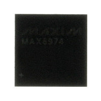
LX1688CPW MICROSEMI, LX1688CPW Datasheet - Page 2

LX1688CPW
Manufacturer Part Number
LX1688CPW
Description
Manufacturer
MICROSEMI
Datasheet
1.LX1688CPW.pdf
(16 pages)
Specifications of LX1688CPW
Driver Type
CCFL
Operating Supply Voltage (typ)
3.3/5V
Number Of Segments
2
Operating Temperature (min)
0C
Operating Temperature (max)
70C
Operating Temperature Classification
Commercial
Package Type
TSSOP
Pin Count
24
Mounting
Surface Mount
Operating Supply Voltage (min)
3V
Operating Supply Voltage (max)
5.5V
Lead Free Status / RoHS Status
Compliant
Copyright © 2001
Rev. 1.2, 2006-03-09
Supply Voltage (VDD_P, VDD)................................................................................ 6.5V
Digital Inputs ................................................................................... -0.3V to VDD +0.5V
Analog Inputs.................................................................................. –0.1V to VDD +0.5V
Digital Outputs................................................................................. -0.3V to VDD +0.5V
Analog Outputs ................................................................................ -0.1V to VDD +0.5V
Maximum Operating Junction Temperature ............................................................150°C
Storage Temperature................................................................................. -65°C to 150°C
Peak Package Solder Reflow Temp. (40 seconds max. exposure) ................260°C(+0.-5)
Note 1: Exceeding these ratings could cause damage to the device. All voltages are with
respect to Ground. Currents are positive into, negative out of the specified terminal.
Junction Temperature Calculation: T
The θ
above assume no ambient airflow.
PW
PHA_SYNC
Pin Name
RMP_RST
THERMAL RESISTANCE
ENABLE
CPWM1
CPWM2
BEPOL
VSS_P
BRITE
CPOR
A
VSS
I_R
JA
OUT
TM
numbers are guidelines for the thermal performance of the device/pc-board system. All of the
Plastic TSSOP 24-Pin
A B S O L U T E M A X I M U M R A T I N G S
If SLAVE= “0”, PHA_SYNC is a CMOS output; if
SLAVE = “1”, it is a CMOS input that make the
A
Output Driver A
Connects to dedicated GND for Aout and Bout
Drivers
Connects to analog GND
Tri-mode input pin to control the polarity of the
ENABLE and BRITE signal
Analog/PWM input for brightness control
Connects an external capacitor C
is used for setting power-up reset pulse width.
Used to enable or disable the chip
Connects to external resistor R
setting for internal oscillator
Connects to external capacitor C
integrating an external digital PWM signal for
analog dimming
Connects to external capacitor C
integrating an external digital PWM signal for
analog dimming.
If SLAVE = “0”, RMP_RST is a CMOS output; if
SLAVE = “1”, it is a CMOS input that locks the
ramp oscillation frequency to the master clock
OUT
/B
11861 Western Avenue, Garden Grove, CA. 92841, 714-898-8121, Fax: 714-893-2570
OUT
-
phase synchronous with the master
JUNCTION TO
T H E R M A L D A T A
J
= T
Description
A
+ (P
F U N C T I O N A L P I N D E S C R I P T I O N
D
x θ
A
JA
MBIENT
).
I
; for bias current
PWM
PWM
POR
Integrated Products Division
, used for
, used for
to VDD and
, θ
®
Microsemi
JA
RangeMAX™
Pin Name
VDDSW
VCOMP
OLSNS
VDD_P
ICOMP
SLAVE
FAULT
TRI_C
VSNS
ISNS
B
VDD
Multiple Lamp CCFL Controller
100°C/W
OUT
P
RODUCTION
Output Driver B
Connects to dedicated VDD for Aout and Bout
Drivers
Connects to analog VDD
Switchable VDD output controlled by ENABLE
Connects to external capacitor C
Analog input to detect open-lamp condition
Analog input from lamp current, has built-in 300mv
offset
Current error Amp’s output; connects to external
capacitor C
Voltage error Amp’s output; connects to external
capacitor C
Analog input from transformer output voltage
Input control pin for setting the IC either in Master
or Slave mode; “1” for slave mode and “0” for
master mode.
Digital output to indicate maximum number of lamp
striking attempts has occurred without lamp
ignition.
PHA_SYNC
RoHS / Pb-free 100% matte Tin Lead Finish
ICOMP
VCOMP
RMP_RST
ENABLE
D
CPWM1
CPWM2
BEPOL
VSS_P
P A C K A G E P I N O U T
BRITE
CPOR
ATA
A
VSS
I_R
, can be used for soft-start
OUT
Description
S
HEET
10
11
12
1
2
3
4
5
6
7
8
9
PW P
(Top View)
ACKAGE
TRI
24
23
22
21
20
19
18
17
16
15
14
13
LX1688
B
VDD_P
VDD
VDDSW
TRI_C
OLSNS
ISNS
ICOMP
VCOMP
VSNS
SLAVE
FAULT
OUT
Page 2


