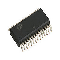
STK11C88-N35 Cypress Semiconductor Corp, STK11C88-N35 Datasheet - Page 2

STK11C88-N35
Manufacturer Part Number
STK11C88-N35
Description
Manufacturer
Cypress Semiconductor Corp
Type
NVSRAMr
Datasheet
1.STK11C88-N35.pdf
(9 pages)
Specifications of STK11C88-N35
Word Size
8b
Organization
32Kx8
Density
256Kb
Interface Type
Parallel
Access Time (max)
35ns
Operating Supply Voltage (typ)
5V
Package Type
SOIC
Operating Temperature Classification
Commercial
Operating Supply Voltage (max)
5.5V
Operating Supply Voltage (min)
4.5V
Operating Temp Range
0C to 70C
Pin Count
28
Mounting
Surface Mount
Supply Current
80mA
Lead Free Status / RoHS Status
Not Compliant
STK11C88
July 1999
ABSOLUTE MAXIMUM RATINGS
Voltage on Input Relative to V
Voltage on DQ
Temperature under Bias . . . . . . . . . . . . . . . . . . . . . –55 C to 125 C
Storage Temperature . . . . . . . . . . . . . . . . . . . . . . . –65 C to 150 C
Power Dissipation . . . . . . . . . . . . . . . . . . . . . . . . . . . . . . . . . . . . 1W
DC Output Current (1 output at a time, 1s duration) . . . . . . . . 15mA
DC CHARACTERISTICS
Note b: The STK11C88-20 requires V
Note c: I
Note d: I
Note e: E V
AC TEST CONDITIONS
CAPACITANCE
Note f:
Input Pulse Levels . . . . . . . . . . . . . . . . . . . . . . . . . . . . . . . 0V to 3V
Input Rise and Fall Times
Input and Output Timing Reference Levels . . . . . . . . . . . . . . . 1.5V
Output Load . . . . . . . . . . . . . . . . . . . . . . . . . . . . . . . . . See Figure 1
SYMBOL
SYMBOL
I
I
I
I
I
I
I
V
V
V
V
T
C
C
CC 1
CC 2
CC 3
SB 1
SB 2
ILK
OLK
A
IH
IL
OH
OL
IN
OUT
e
e
c
d
c
These parameters are guaranteed but not tested.
CC 1
CC
2
and I
is the average current required for the duration of the
Average V
Average V
Average V
5V, 25°C, Typical
Average V
(Standby, Cycling TTL Input Levels)
V
(Standby, Stable CMOS Input Levels)
Input Leakage Current
Off-State Output Leakage Current
Input Logic “1” Voltage
Input Logic “0” Voltage
Output Logic “1” Voltage
Output Logic “0” Voltage
Operating Temperature
IH
0-7
CC
Input Capacitance
Output Capacitance
will not produce standby current levels until any nonvolatile cycle in progress has timed out.
PARAMETER
. . . . . . . . . . . . . . . . . . . . . . –0.5V to (V
CC 3
Standby Current
are dependent on output loading and cycle rate. The specified values are obtained with outputs unloaded.
CC
CC
CC
CC
PARAMETER
Current
f
Current
Current during STORE
Current at t
SS
. . . . . . . . . . –0.6V to (V
(T
AVAV
A
CC
MAX
= 25 C, f = 1.0MHz)
5
7
= 5.0V 5% supply to operate at specified speed.
= 200ns
UNITS
pF
pF
V
SS
MIN
COMMERCIAL
2.2
2.4
a
CONDITIONS
0
– .5
CC
CC
V = 0 to 3V
V = 0 to 3V
+ 0.5V)
+ 0.5V)
V
STORE
CC
MAX
5ns
110
750
0.8
0.4
97
80
70
10
35
30
25
22
70
3
1
5
+ .5
5-2
cycle (t
Note a: Stresses greater than those listed under “Absolute Maximum
V
SS
MIN
–40
INDUSTRIAL
2.2
2.4
– .5
STORE
Ratings” may cause permanent damage to the device. This is a
stress rating only, and functional operation of the device at condi-
tions above those indicated in the operational sections of this
specification is not implied. Exposure to absolute maximum rat-
ing conditions for extended periods may affect reliability.
V
OUTPUT
CC
MAX
N/A
100
N/A
750
) .
0.8
0.4
85
70
10
31
26
23
85
3
1
5
+ .5
UNITS
Figure 1: AC Output Loading
mA
mA
mA
mA
mA
mA
mA
mA
mA
mA
V
V
V
V
C
A
A
A
255 Ohms
t
t
t
t
All Inputs Don’t Care, V
W
All Others Cycling, CMOS Levels
t
t
t
t
E
All Others V
V
V
V
V
All Inputs
All Inputs
I
I
AVAV
AVAV
AVAV
AVAV
AVAV
AVAV
AVAV
AVAV
OUT
OUT
CC
IN
CC
IN
= V
(V
= V
(V
= max
= max
= – 4mA
= 8mA
= 35ns
= 25ns, E
= 20ns
= 25ns
= 45ns
= 20ns, E
= 35ns, E
= 45ns, E
CC
CC
SS
SS
(V
– 0.2V)
- 0.2V)
to V
to V
CC
IN
CC
CC
0.2V or
NOTES
, E or G
V
= 5.0V
V
V
V
IH
IH
IH
IH
5.0V
CC
480 Ohms
(V
30 pF
INCLUDING
SCOPE AND
FIXTURE
= max
V
CC
IH
– 0.2V)
10%)
b


