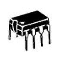
CAT93C46RLI-G ON Semiconductor, CAT93C46RLI-G Datasheet

CAT93C46RLI-G
Specifications of CAT93C46RLI-G
Related parts for CAT93C46RLI-G
CAT93C46RLI-G Summary of contents
Page 1
... CAT93C46R SK DI GND Figure 1. Functional Symbol *For additional information on our Pb−Free strategy and soldering details, please download the ON Semiconductor Soldering and Mounting Techniques Reference Manual, SOLDERRM/D. © Semiconductor Components Industries, LLC, 2009 October, 2009 − Rev. 7 CASE 646AA SOIC−8 V SUFFIX ...
Page 2
Table 1. ABSOLUTE MAXIMUM RATINGS Parameter Storage Temperature Voltage on Any Pin with Respect to Ground (Note 1) Stresses exceeding Maximum Ratings may damage the device. Maximum Ratings are stress ratings only. Functional operation above the Recommended Operating Conditions is ...
Page 3
Table 4. PIN CAPACITANCE Symbol C (Note 4) Output Capacitance (DO) OUT C (Note 4) Input Capacitance (CS, SK, DI, ORG These parameters are tested initially and after a design or process change that affects the parameter according ...
Page 4
Table 8. INSTRUCTION SET Instruction Start Bit Opcode READ 1 10 ERASE 1 11 WRITE 1 01 EWEN 1 00 EWDS 1 00 ERAL 1 00 WRAL 1 00 Device Operation The CAT93C46R is a 1024−bit nonvolatile memory intended for ...
Page 5
SK t VALID DI t CSS HIGH− HIGH− SKHI SKLOW DIS VALID t DIS ...
Page 6
ENABLE = 11 DISABLE = 00 Write After receiving a WRITE command, address and the data, the CS (Chip Select) pin must be deselected for a minimum of t (See Design Note for ...
Page 7
HIGH− N− HIGH−Z Figure 7. Erase Instruction Timing 0 t ...
Page 8
PIN # 1 IDENTIFICATION D TOP VIEW SIDE VIEW Notes: (1) All dimensions are in millimeters. (2) Complies with JEDEC MS-001. PACKAGE DIMENSIONS PDIP−8, 300 mils CASE 646AA−01 ISSUE A SYMBOL ...
Page 9
PIN # 1 IDENTIFICATION TOP VIEW SIDE VIEW Notes: (1) All dimensions are in millimeters. Angles in degrees. (2) Complies with JEDEC MS-012. PACKAGE DIMENSIONS SOIC 8, 150 mils CASE 751BD−01 ISSUE O SYMBOL ...
Page 10
PIN#1 IDENTIFICATION TOP VIEW SIDE VIEW Notes: (1) All dimensions are in millimeters. Angles in degrees. (2) Complies with EIAJ EDR-7320. PACKAGE DIMENSIONS SOIC−8, 208 mils CASE 751BE−01 ISSUE O SYMBOL ...
Page 11
E1 e TOP VIEW SIDE VIEW Notes: (1) All dimensions are in millimeters. Angles in degrees. (2) Complies with JEDEC MO-153. PACKAGE DIMENSIONS TSSOP8, 4.4x3 CASE 948AL−01 ISSUE O SYMBOL MIN A A1 0.05 A2 ...
Page 12
D E PIN#1 INDEX AREA TOP VIEW SYMBOL MIN NOM A 0.70 0.75 A1 0.00 0.02 A2 0.45 0.55 A3 0.20 REF b 0.20 0.25 D 1.90 2.00 D2 1.30 1.40 E 2.90 3.00 E2 1.20 1.30 e 0.50 TYP ...
Page 13
... W: SOIC, JEDEC X: SOIC, EIAJ (Note 11) Y: TSSOP VP2: TDFN ( mm) ORDERING INFORMATION Orderable Part Numbers CAT93C46RLI−G CAT93C46RVI−GT3 CAT93C46RWI−GT3 CAT93C46RXI−T2 CAT93C46RYI−GT3 CAT93C46RVP2IGT3 (Note 13) 8. The device used in the above example is a CAT93C46RVI−GT3 (SOIC, Industrial Temperature, NiPdAu, Tape & Reel). ...


