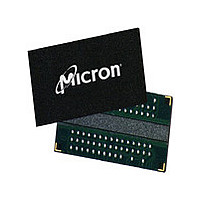
MT47H128M16HG-3:A Micron Technology Inc, MT47H128M16HG-3:A Datasheet - Page 31

MT47H128M16HG-3:A
Manufacturer Part Number
MT47H128M16HG-3:A
Description
Manufacturer
Micron Technology Inc
Type
DDR2 SDRAMr
Datasheet
1.MT47H128M16HG-3A.pdf
(134 pages)
Specifications of MT47H128M16HG-3:A
Organization
128Mx16
Address Bus
17b
Access Time (max)
450ps
Maximum Clock Rate
667MHz
Operating Supply Voltage (typ)
1.8V
Package Type
FBGA
Operating Temp Range
0C to 70C
Operating Supply Voltage (max)
1.9V
Operating Supply Voltage (min)
1.7V
Supply Current
275mA
Pin Count
84
Mounting
Surface Mount
Operating Temperature Classification
Commercial
Lead Free Status / RoHS Status
Compliant
Available stocks
Company
Part Number
Manufacturer
Quantity
Price
Part Number:
MT47H128M16HG-3:A
Manufacturer:
MICRON
Quantity:
20 000
Table 11: DDR2 I
Notes 1–7 apply to the entire table
PDF: 09005aef824f87b6
2gbddr2.pdf – Rev. F 12/10 EN
Parameter/Condition
Operating one bank active-precharge cur-
rent:
MIN (I
commands; Address bus inputs are switching; Da-
ta bus inputs are switching
Operating one bank active-read-precharge
current: Iout = 0mA; BL = 4, CL = CL (I
t
(I
between valid commands; Address bus inputs are
switching; Data pattern is same as I
Precharge power-down current: All banks
idle;
and address bus inputs are stable; Data bus in-
puts are floating
Precharge quiet standby current: All banks
idle;
er control and address bus inputs are stable; Data
bus inputs are floating
Precharge standby current: All banks idle;
=
trol and address bus inputs are switching; Data
bus inputs are switching
Active power-down current: All banks open;
t
dress bus inputs are stable; Data bus inputs are
floating
Active standby current: All banks open;
t
CKE is HIGH, CS# is HIGH between valid com-
mands; Other control and address bus inputs are
switching; Data bus inputs are switching
Operating burst write current: All banks
open, continuous burst writes; BL = 4, CL = CL
(I
(I
tween valid commands; Address bus inputs are
switching; Data bus inputs are switching
Operating burst read current: All banks open,
continuous burst reads, I
CL (I
(I
tween valid commands; Address bus inputs are
switching; Data bus inputs are switching
CK =
CK =
CK (I
DD
DD
DD
DD
t
CK (I
),
), AL = 0;
),
),
DD
t
t
DD
CK =
t
CK =
t
t
t
t
t
DD
RCD =
RP =
RP =
CK =
CK (I
CK (I
), AL = 0;
DD
),
); CKE is HIGH, CS# is HIGH between valid
); CKE is HIGH, CS# is HIGH; Other con-
t
RAS =
t
t
DD
DD
CK (I
t
t
CK (I
t
RP (I
RP (I
CK (I
t
t
); CKE is LOW; Other control and ad-
),
RCD (I
CK =
t
DD
RC =
DD
t
DD
DD
t
CK =
DD
RAS MAX (I
); CKE is HIGH, CS# is HIGH; Oth-
); CKE is LOW; Other control
); CKE is HIGH, CS# is HIGH be-
); CKE is HIGH, CS# is HIGH be-
t
),
DD
CK (I
DD
t
t
RC (I
RC =
); CKE is HIGH, CS# is HIGH
t
CK (I
Specifications and Conditions (Die Revision C)
DD
OUT
DD
),
t
DD
RC (I
t
),
= 0mA; BL = 4, CL =
DD
RAS =
),
t
),
RAS =
t
DD
RAS =
t
RP =
),
DD4W
t
RAS MAX
t
RAS =
t
DD
RAS MIN
t
t
RP (I
RAS MAX
), AL = 0;
t
t
CK =
DD
RAS
t
);
CK
Symbol
I
I
I
I
I
I
I
I
DD3Pf
DD3Ps
DD4W
I
I
DD2Q
DD2N
DD3N
DD2P
DD4R
DD0
DD1
31
Electrical Specifications – I
Configuration
Slow PDN exit
Fast PDN exit
MR[12] = 0
MR[12] = 1
x4, x8, x16
x4, x8
x4, x8
x4, x8
x4, x8
x4, x8
x4, x8
x4, x8
x16
x16
x16
x16
x16
x16
x16
Micron Technology, Inc. reserves the right to change products or specifications without notice.
2Gb: x4, x8, x16 DDR2 SDRAM
-187E
tdb
tbd
tbd
tbd
tbd
tbd
tbd
tbd
tbd
tbd
tbd
tbd
tbd
tbd
tbd
tbd
tbd
-25E/-25
115
125
150
235
150
235
80
95
12
35
50
40
55
30
14
50
70
© 2006 Micron Technology, Inc. All rights reserved.
DD
-3/-3E
110
120
130
200
130
200
75
90
12
30
45
35
50
25
14
45
65
Parameters
Units
mA
mA
mA
mA
mA
mA
mA
mA
mA


