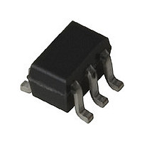
TSDF72830YS-GS08 Vishay, TSDF72830YS-GS08 Datasheet - Page 3

TSDF72830YS-GS08
Manufacturer Part Number
TSDF72830YS-GS08
Description
Manufacturer
Vishay
Datasheet
1.TSDF72830YS-GS08.pdf
(8 pages)
Specifications of TSDF72830YS-GS08
Mounting
Surface Mount
Pin Count
6
Lead Free Status / RoHS Status
Compliant
Electrical DC Characteristics
T
Amplifier 1
Following data are valid for operating amplifier 1 (pin 1, 6, 2, 5) which is optimized for VHF applications
Amplifier 2
Following data are valid for operating amplifier 2 (pin 3, 4, 2, 5) which is optimized for UHF applications
Document Number 85176
Rev. 1.1, 02-May-05
Gate 1 - source breakdown
voltage
Gate 2 - source breakdown
voltage
Gate 1 - source leakage current + V
Gate 2 - source leakage current ± V
Drain - source operating current V
Gate 2 - source cut-off voltage
Drain - source breakdown
voltage
Gate 1 - source breakdown
voltage
Gate 1 - source leakage current + V
Gate 2 - source leakage current ± V
Drain - source operating current V
Gate 1 - source cut-off voltage
Gate 2 - source cut-off voltage
amb
= 25 °C, unless otherwise specified
Parameter
Parameter
+ I
± I
Gate 1 = nc
V
I
I
+ I
± I
R
V
V
I
D
D
D
DS
DS
DS
DS
DS
G1
G1S
G2S
= 20 μA
= 10 μA, V
G1S
G2S
= 20 μA
G1S
G2S
G1S
G2S
= V
= V
= V
= V
= 100 kΩ
= 5 V, V
= 10 mA, V
= 10 mA, V
= 10 mA, V
= 10 mA, V
= 5 V, V
= 5 V, V
= 5 V, V
= 5 V, V
RG1
RG1
RG1
RG1
Test condition
Test condition
= 5 V, R
= 5 V, V
= 5 V, Gate 1 = nc,
= 5 V, V
G2S
G2S
G2S
G1S
G2S
G1S
= 4, I
= V
G2S
G1S
G2S
G1S
G1
= V
= V
= V
= V
G2S
G2S
G1S
D
= V
= V
= V
= V
=100 kΩ,
DS
DS
DS
DS
= 20 μA
= 4 V,
= 4 V,
= 0
DS
DS
DS
DS
= 0
= 0
= 0
= 0
= 0 + V
= 0 ± V
= 0 + V
= 0 ± V
V
V
V
V
Symbol
+ I
± I
Symbol
+ I
± I
G2S(OFF)
G1S(OFF)
G2S(OFF)
(BR)DSS
(BR)G1SS
(BR)G2SS
(BR)G1SS
(BR)G2SS
I
I
DSP
DSO
G1SS
G2SS
G1SS
G2SS
Min
Min
0.3
0.3
0.3
15
7
7
8
7
7
8
TSDF72830YS
Vishay Semiconductors
Typ.
Typ.
13
12
Max
Max
1.2
1.0
1.2
10
10
50
20
17
10
10
20
20
17
www.vishay.com
Unit
Unit
mA
mA
μA
nA
nA
nA
V
V
V
V
V
V
V
V
3


