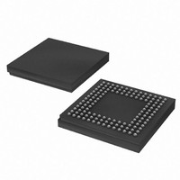
XC3S500E-4CPG132C Xilinx Inc, XC3S500E-4CPG132C Datasheet - Page 230

XC3S500E-4CPG132C
Manufacturer Part Number
XC3S500E-4CPG132C
Description
FPGA Spartan®-3E Family 500K Gates 10476 Cells 572MHz 90nm (CMOS) Technology 1.2V 132-Pin CSBGA
Manufacturer
Xilinx Inc
Series
Spartan™-3Er
Datasheet
1.XC3S100E-4VQG100C.pdf
(233 pages)
Specifications of XC3S500E-4CPG132C
Package
132CSBGA
Family Name
Spartan®-3E
Device Logic Cells
10476
Device Logic Units
1164
Device System Gates
500000
Number Of Registers
9312
Maximum Internal Frequency
572 MHz
Typical Operating Supply Voltage
1.2 V
Maximum Number Of User I/os
92
Ram Bits
368640
Number Of Logic Elements/cells
10476
Number Of Labs/clbs
1164
Total Ram Bits
368640
Number Of I /o
92
Number Of Gates
500000
Voltage - Supply
1.14 V ~ 1.26 V
Mounting Type
Surface Mount
Operating Temperature
0°C ~ 85°C
Package / Case
132-TFBGA, CSPBGA
Lead Free Status / RoHS Status
Lead free / RoHS Compliant
For Use With
122-1536 - KIT STARTER SPARTAN-3E
Lead Free Status / RoHS Status
Lead free / RoHS Compliant
Other names
122-1484
Available stocks
Company
Part Number
Manufacturer
Quantity
Price
Company:
Part Number:
XC3S500E-4CPG132C
Manufacturer:
Xilinx Inc
Quantity:
10 000
Part Number:
XC3S500E-4CPG132C
Manufacturer:
XILINX/赛灵思
Quantity:
20 000
- Current page: 230 of 233
- Download datasheet (6Mb)
Pinout Descriptions
Table 154: FG484 Package Pinout (Continued)
User I/Os by Bank
Table 155
distributed between the four I/O banks on the FG484 pack-
age.
Table 155: User I/Os Per Bank for the XC3S1600E in the FG484 Package
Footprint Migration Differences
The XC3S1600E FPGA is the only Spartan-3E device
offered in the FG484 package.
230
Notes:
1.
2.
VCCAUX VCCAUX
Top
Right
Bottom
Left
TOTAL
VCCINT
VCCINT
VCCINT
VCCINT
VCCINT
VCCINT
VCCINT
VCCINT
VCCINT
Bank
Package
Some VREF and CLK pins are on INPUT pins.
The eight global clock pins in this bank have optional functionality during configuration and are counted in the DUAL column.
Edge
indicates how the 304 available user-I/O pins are
VCCINT
VCCINT
VCCINT
VCCINT
VCCINT
VCCINT
VCCINT
VCCINT
VCCINT
I/O Bank
XC3S1600E
Pin Name
0
1
2
3
Maximum
376
I/O
94
94
94
94
FG484
W11
Ball
K11
K13
J10
L10
L11
L12
L14
M9
K9
VCCAUX
VCCINT
VCCINT
VCCINT
VCCINT
VCCINT
VCCINT
VCCINT
VCCINT
VCCINT
Type
214
I/O
56
50
45
63
www.xilinx.com
Table 154: FG484 Package Pinout (Continued)
VCCINT
VCCINT
VCCINT
VCCINT
VCCINT
VCCINT
VCCINT
INPUT
Bank
22
16
18
16
72
All Possible I/O Pins by Type
VCCINT
VCCINT
VCCINT
VCCINT
VCCINT
VCCINT
VCCINT
DUAL
XC3S1600E
Pin Name
21
24
46
1
0
DS312-4 (v3.8) August 26, 2009
VREF
28
7
7
7
7
(1)
Product Specification
FG484
M11
M12
M13
Ball
N10
N12
N14
P13
CLK
0
0
VCCINT
VCCINT
VCCINT
VCCINT
VCCINT
VCCINT
VCCINT
16
8
8
(2)
(2)
Type
(1)
R
Related parts for XC3S500E-4CPG132C
Image
Part Number
Description
Manufacturer
Datasheet
Request
R

Part Number:
Description:
IC SPARTAN-3E FPGA 500K 320FBGA
Manufacturer:
Xilinx Inc
Datasheet:

Part Number:
Description:
IC FPGA SPARTAN-3E 500K 208-PQFP
Manufacturer:
Xilinx Inc
Datasheet:

Part Number:
Description:
IC FPGA SPARTAN-3E 500K 132CSBGA
Manufacturer:
Xilinx Inc
Datasheet:

Part Number:
Description:
IC FPGA SPARTAN-3E 500K 256FTBGA
Manufacturer:
Xilinx Inc
Datasheet:

Part Number:
Description:
IC FPGA SPARTAN-3E 500K 256FTBGA
Manufacturer:
Xilinx Inc
Datasheet:

Part Number:
Description:
IC FPGA SPARTAN-3E 500K 320-FBGA
Manufacturer:
Xilinx Inc
Datasheet:

Part Number:
Description:
IC FPGA SPARTAN 3E 320FBGA
Manufacturer:
Xilinx Inc
Datasheet:

Part Number:
Description:
FPGA Spartan®-3E Family 500K Gates 10476 Cells 572MHz 90nm (CMOS) Technology 1.2V 256-Pin FTBGA
Manufacturer:
Xilinx Inc
Datasheet:

Part Number:
Description:
FPGA Spartan®-3E Family 500K Gates 10476 Cells 572MHz 90nm (CMOS) Technology 1.2V 208-Pin PQFP
Manufacturer:
Xilinx Inc
Datasheet:

Part Number:
Description:
FPGA Spartan®-3E Family 500K Gates 10476 Cells 572MHz 90nm (CMOS) Technology 1.2V 208-Pin PQFP
Manufacturer:
Xilinx Inc
Datasheet:

Part Number:
Description:
FPGA Spartan®-3E Family 500K Gates 10476 Cells 572MHz 90nm (CMOS) Technology 1.2V 256-Pin FTBGA
Manufacturer:
Xilinx Inc
Datasheet:

Part Number:
Description:
FPGA Spartan-3E Family 500K Gates 10476 Cells 572MHz 90nm (CMOS) Technology 1.2V 320-Pin FBGA
Manufacturer:
Xilinx Inc
Datasheet:

Part Number:
Description:
IC FPGA SPARTAN-3E 500K 100-VQFP
Manufacturer:
Xilinx Inc
Datasheet:

Part Number:
Description:
IC FPGA SPARTAN-3E 500K 132CSBGA
Manufacturer:
Xilinx Inc
Datasheet:

Part Number:
Description:
IC FPGA SPARTAN-3E 500K 320-FBGA
Manufacturer:
Xilinx Inc
Datasheet:


