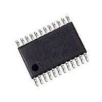
AD5204BRU10-REEL7 Analog Devices Inc, AD5204BRU10-REEL7 Datasheet - Page 12

AD5204BRU10-REEL7
Manufacturer Part Number
AD5204BRU10-REEL7
Description
Manufacturer
Analog Devices Inc
Datasheet
1.AD5204BRU10-REEL7.pdf
(20 pages)
Specifications of AD5204BRU10-REEL7
Number Of Elements
4
# Of Taps
256
Resistance (max)
10KOhm
Power Supply Requirement
Single/Dual
Interface Type
Serial (3-Wire/SPI)
Single Supply Voltage (typ)
3/5V
Dual Supply Voltage (typ)
±2.5V
Single Supply Voltage (min)
2.7V
Single Supply Voltage (max)
5.5V
Dual Supply Voltage (min)
±2.3V
Dual Supply Voltage (max)
±2.7V
Operating Temp Range
-40C to 85C
Operating Temperature Classification
Industrial
Mounting
Surface Mount
Pin Count
24
Lead Free Status / RoHS Status
Not Compliant
Available stocks
Company
Part Number
Manufacturer
Quantity
Price
Company:
Part Number:
AD5204BRU10-REEL7
Manufacturer:
SAMSUNG
Quantity:
1 400
AD5204/AD5206
OPERATION
The AD5204 provides a 4-channel, 256-position digitally
controlled VR device, and the AD5206 provides a 6-channel,
256-position digitally controlled VR device. Changing the pro-
grammed VR settings is accomplished by clocking an 11-bit
serial data-word into the SDI pin. The format of this data-word
is three address bits, MSB first, followed by eight data bits, MSB
first. Table 6 provides the serial register data-word format.
Table 6. Serial Data-Word Format
B10
A2
MSB
2
See Table 10 for the AD5204/AD5206 address assignments to
decode the location of the VR latch receiving the serial register
data in Bit B7 through Bit B0. The VR outputs can be changed
one at a time in random sequence. The AD5204 presets to
midscale by asserting the PR pin, simplifying fault condition
recovery at power up. Both parts have an internal power-on
preset that places the wiper in a preset midscale condition at
power on. In addition, the AD5204 contains a power shutdown pin
( SHDN ) that places the RDAC in a zero power consumption
state, where terminals Ax are open circuited and wipers Wx are
10
Address
B9
A1
B8
A0
LSB
2
8
B7
D7
MSB
2
7
B6
D6
B5
D5
B4
D4
Data
B3
D3
B2
D2
B1
D1
Rev. C | Page 12 of 20
B0
D0
LSB
2
0
connected to terminals Bx, resulting in only leakage currents
being consumed in the VR structure. In shutdown mode, the
VR latch settings are maintained so that the VR settings return
to their previous resistance values when the device is returned
to operational mode from power shutdown.
SHDN
Figure 21. AD5204/AD5206 Equivalent RDAC Circuit
D7
D6
D5
D4
D3
D2
D1
D0
DECODER
LATCH
RDAC
AND
R
R
R
R
S
S
S
S
Ax
Wx
Bx


