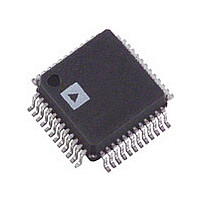
ADV7172KST Analog Devices Inc, ADV7172KST Datasheet - Page 9

ADV7172KST
Manufacturer Part Number
ADV7172KST
Description
Manufacturer
Analog Devices Inc
Datasheet
1.ADV7172KST.pdf
(60 pages)
Specifications of ADV7172KST
Number Of Dac's
6
Adc/dac Resolution
10b
Screening Level
Commercial
Package Type
LQFP
Pin Count
48
Lead Free Status / RoHS Status
Not Compliant
Available stocks
Company
Part Number
Manufacturer
Quantity
Price
Company:
Part Number:
ADV7172KST
Manufacturer:
SUN
Quantity:
5 000
Company:
Part Number:
ADV7172KST
Manufacturer:
ADI
Quantity:
850
Part Number:
ADV7172KST
Manufacturer:
ADI/亚德诺
Quantity:
20 000
Company:
Part Number:
ADV7172KSTZ
Manufacturer:
AD
Quantity:
80
Part Number:
ADV7172KSTZ
Manufacturer:
ADI/亚德诺
Quantity:
20 000
Company:
Part Number:
ADV7172KSTZ-REEL
Manufacturer:
Analog Devices Inc
Quantity:
10 000
ABSOLUTE MAXIMUM RATINGS
V
Voltage on Any Digital Input Pin . GND – 0.5 V to V
Storage Temperature (T
Junction Temperature (T
Lead Temperature (Soldering, 10 sec) . . . . . . . . . . . . . . 260°C
Analog Outputs to GND
NOTES
1
2
CAUTION
ESD (electrostatic discharge) sensitive device. Electrostatic charges as high as 4000 V readily
accumulate on the human body and test equipment and can discharge without detection.
Although the ADV7172/ADV7173 features proprietary ESD protection circuitry, permanent
damage may occur on devices subjected to high-energy electrostatic discharges. Therefore,
proper ESD precautions are recommended to avoid performance degradation or loss of
functionality.
Stresses above those listed under Absolute Maximum Ratings may cause permanent
Analog output short circuit to any power supply or common can be of an
damage to the device. This is a stress rating only; functional operation of the device
at these or any other conditions above those listed in the operational sections of this
specification is not implied. Exposure to absolute maximum rating conditions for
extended periods may affect device reliability.
indefinite duration.
AA
to GND . . . . . . . . . . . . . . . . . . . . . . . . . . . . . . . . . . . 7 V
CSO HSO
GND
V
V
AA
P0
P1
P2
P3
P4
P5
P6
P7
AA
10
11
12
1
2
3
4
5
6
7
8
9
48 47 46 45 44
13 14 15 16 17 18 19 20 21 22 23 24
PIN CONFIGURATION
PIN 1
IDENTIFIER
ADV7172/ADV7173
S
2
) . . . . . . . . . . . . . . –65°C to +150°C
J
) . . . . . . . . . . . . . . . . . . . . . . 150°C
(Not to Scale)
. . . . . . . . . . . GND – 0.5 V to V
TOP VIEW
43 42 41 40
1
39 38 37
36
35
34
33
32
31
30
29
28
27
26
25
COMP1
DAC A
V
DAC B
V
GND
V
DAC C
DAC D
V
GND
DAC E
AA
AA
AA
AA
AA
+ 0.5 V
AA
PACKAGE THERMAL PERFORMANCE
The 48-lead LQFP package is used for this device. The junc-
tion-to-ambient (θ
layer PCB is 54.6°C/W. The junction-to-case thermal resistance
(θ
To reduce power consumption when using this part the user is
advised to run the part on a 3.3 V supply, turn off any unused
DACs. However, if 5 V operation is required the user can enable
Low Power mode by setting MR16 to a Logic 1. Another alter-
native way to further reduce power is to use external buffers that
dramatically reduce the DAC currents, the current can be low-
ered to as low as 5 mA (see AN-551 and Appendix 8 for more
details) from a nominal value of 36 mA.
The user must at all times stay below the maximum junction
temperature of 110°C. The following equation shows how to
calculate this junction temperature:
where
I
powered-on DAC).
Model
ADV7172KST 0°C to 70°C
ADV7173KST 0°C to 70°C
DAC
JC
) is 16.7°C.
= 10 mA + (sum of the average currents consumed by each
J
unction Temperature = [V
Temperature
Range
JA
) thermal resistance in still air on a four
ORDERING GUIDE
ADV7172/ADV7173
AA
WARNING!
(I
DAC
Package
Description
Plastic Thin
Quad Flatpack
Plastic Thin
Quad Flatpack
+ I
CCT
ESD SENSITIVE DEVICE
) × θ
JA
] 70°C
Package
Option
ST-48
ST-48


