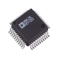
ADV7170KS Analog Devices Inc, ADV7170KS Datasheet - Page 26

ADV7170KS
Manufacturer Part Number
ADV7170KS
Description
Manufacturer
Analog Devices Inc
Datasheet
1.ADV7170KS.pdf
(64 pages)
Specifications of ADV7170KS
Adc/dac Resolution
10b
Screening Level
Industrial
Package Type
MQFP
Pin Count
44
Lead Free Status / RoHS Status
Not Compliant
Available stocks
Company
Part Number
Manufacturer
Quantity
Price
Part Number:
ADV7170KS
Manufacturer:
ADI/亚德诺
Quantity:
20 000
Company:
Part Number:
ADV7170KSU
Manufacturer:
AD
Quantity:
1 364
Part Number:
ADV7170KSU
Manufacturer:
ADI/亚德诺
Quantity:
20 000
Part Number:
ADV7170KSUZ-REEL
Manufacturer:
ADI/亚德诺
Quantity:
20 000
Part Number:
ADV7170KSZ
Manufacturer:
ADI/亚德诺
Quantity:
20 000
ADV7170/ADV7171
POWER-ON RESET
After power-up, it is necessary to execute a reset operation.
A reset occurs on the falling edge of a high-to-low transition
on the RESET pin. This initializes the pixel port so that the pixel
inputs, P7 to P0, are selected. After reset, the ADV7170/
ADV7171 is automatically set up to operate in NTSC mode.
Subcarrier frequency code 21F07C16HEX is loaded into the
subcarrier frequency registers. All other registers, with the
exception of Mode Register 0, are set to 00H. All bits in
Mode Register 0 are set to Logic Level 0, except Bit MR44.
Bit MR44 of Mode Register 4 is set to Logic Level 1. This
enables the 7.5 IRE pedestal.
SCH PHASE MODE
The SCH phase is configured in default mode to reset every
four (NTSC) or eight (PAL) fields to avoid an accumulation of
SCH phase error over time. In an ideal system, zero SCH phase
error would be maintained forever, but in reality, this is
impossible to achieve due to clock frequency variations. This
effect is reduced by the use of a 32-bit DDS, which generates
this SCH.
Resetting the SCH phase every four or eight fields avoids the
accumulation of SCH phase error and results in very minor
SCH phase jumps at the start of the four or eight field sequence.
Resetting the SCH phase should not be done if the video source
does not have stable timing or the ADV7170/ADV7171 are
configured in RTC mode (MR21 = 1 and MR22 = 1). Under
these conditions (unstable video), the subcarrier phase reset
should be enabled (MR22 = 0 and MR21 = 1) but no reset
applied. In this configuration the SCH phase is never reset,
which means the output video tracks the unstable input video.
The subcarrier phase reset, when applied, resets the SCH phase
to Field 0 at the start of the next field (for example, subcarrier
phase reset applied in Field 5 [PAL] on the start of the next field
SCH phase resets to Field 0).
MPU PORT DESCRIPTION
The ADV7170/ADV7171 support a 2-wire, serial (I
compatible) microprocessor bus driving multiple peripherals.
Two inputs, serial data (SDATA), and serial clock (SCLOCK),
carry information between any devices connected to the bus.
Each slave device is recognized by a unique address. The
ADV7170/ADV7171 each have four possible slave addresses for
both read and write operations. These are unique addresses for
each device and are shown in Figure 33 and Figure 34.
The LSB sets either a read or write operation. Logic Level 1
corresponds to a read operation, while Logic Level 0 corre-
sponds to a write operation. A 1 is set by setting the ALSB pin of
the ADV7170/ADV7171 to Logic Level 0 or Logic Level 1.
2
C-
Rev. C | Page 26 of 64
To control the various devices on the bus, the following
protocol must be followed: first, the master initiates a data
transfer by establishing a start condition, defined by a high-to-
low transition on SDATA while SCLOCK remains high. This
indicates that an address/data stream follows. All peripherals
respond to the start condition and shift the next eight bits
(7-bit address + R/RW bit). The bits transfer from MSB down to
LSB. The peripheral that recognizes the transmitted address
responds by pulling the data line low during the ninth clock
pulse. This is known as an acknowledge bit. All other devices
withdraw from the bus at this point and maintain an idle
condition. The idle condition is where the device monitors the
SDATA and SCLOCK lines waiting for the start condition and
the correct transmitted address. The R/RW bit determines the
direction of the data. A Logic Level 0 on the LSB of the first byte
means that the master writes information to the peripheral. A
Logic Level 1 on the LSB of the first byte means the master
reads information from the peripheral.
1
0
1
1
0
Figure 33. ADV7170 Slave Address
0
Figure 34. ADV7171 Slave Address
1
1
0
0
1
1
SET UP BY
SET UP BY
ADDRESS
CONTROL
ADDRESS
CONTROL
ALSB
ALSB
A1
A1
READ/WRITE
READ/WRITE
CONTROL
0
1
CONTROL
0
1
X
WRITE
READ
X
WRITE
READ


