USB3315-CP-TR Standard Microsystems (SMSC), USB3315-CP-TR Datasheet

USB3315-CP-TR

Manufacturer Part Number
USB3315-CP-TR
Description
Manufacturer
Standard Microsystems (SMSC)
Datasheet

Specifications of USB3315-CP-TR

Number Of Transceivers
1
Esd Protection
YeskV
Power Supply Requirement
Triple
Operating Supply Voltage (typ)
Not RequiredV
Package Type
QFN
Operating Temperature Classification
Industrial
Operating Supply Voltage (max)
Not RequiredV
Operating Supply Voltage (min)
Not RequiredV
Dual Supply Voltage (typ)
1.8/2.5/3.3/5V
Mounting
Surface Mount
Operating Temperature (max)
85C
Operating Temperature (min)
-40C
Lead Free Status / RoHS Status
Compliant
PRODUCT FEATURES
SMSC USB3315
USB-IF “Hi-Speed” compliant to the Universal Serial
Interface compliant with the ULPI Specification
1.8V to 3.3V IO Voltage (+/- 10%)
SMSC flexPWR
Supports FS pre-amble for FS hubs with a LS device
Supports HS SOF and LS keep-alive pulse
Includes full support for the optional On-The-Go
Supports the OTG Host Negotiation Protocol (HNP)
Allows host to turn VBUS off to conserve battery
Support OTG monitoring of VBUS levels with internal
“Wrapper-less” design for optimal timing performance
Internal 5V cable short-circuit protection of ID, DP
24MHz Reference Clock operation
Internal low jitter PLL for 480MHz Hi-Speed USB
Internal detection of the value of resistance to ground
Integrated battery to 3.3V LDO regulator
Integrated ESD protection circuits
Bus Specification Rev 2.0
revision 1.1 as a Single Data Rate (SDR) PHY
— Low current design ideal for battery powered
— “Sleep” mode tri-states all ULPI pins and places the
attached (UTMI+ Level 3)
(OTG) protocol detailed in the On-The-Go
Supplement Revision 1.0a specification
and Session Request Protocol (SRP)
power in OTG applications
comparators
and design ease
— Low Latency Hi-Speed Receiver (43 Hi-Speed clocks
and DM lines to VBUS or ground
— 0 to 3.6V input drive tolerant
— Able to accept “noisy” clock sources
operation
on the ID pin
— 2.2uF bypass capacitor
— 100mV dropout voltage
— Up to +-15kV without any external devices
applications
part in a low current state
Max) allows use of legacy UTMI Links with a ULPI
bridge
TM
Technology
PRODUCT PREVIEW
Hi-Speed USB Transceiver
with 1.8V-3.3V ULPI Interface -
24MHz Reference Clock
Applications
The USB3315 is targeted for any application where a Hi-
Speed USB connection is desired and when board
space, power, and interface pins must be minimized.
The USB3315 is well suited for:
Carkit UART mode for non-USB serial data transfers
Industrial Operating Temperature -40°C to +85°C
Packaging Options
Cell Phones
PDAs
MP3 Players
GPS Personal Navigation
Scanners
External Hard Drives
Digital Still and Video Cameras
Portable Media Players
Entertainment Devices
Printers
Set Top Boxes
Video Record/Playback Systems
IP and Video Phones
Gaming Consoles
POS Terminals
— 24 pin QFN lead-free RoHS compliant package
USB3315
(4 x 4 x 0.90 mm height)
Revision 1.3 (11-02-07)
Data Brief

Related parts for USB3315-CP-TR

USB3315-CP-TR Summary of contents

Page 1

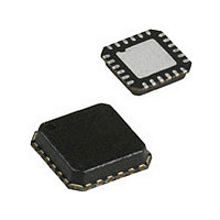
... Packaging Options — 24 pin QFN lead-free RoHS compliant package ( 0.90 mm height) Applications The USB3315 is targeted for any application where a Hi- Speed USB connection is desired and when board space, power, and interface pins must be minimized. The USB3315 is well suited for: Cell Phones ...

Page 2

... USB3315-CP-TR FOR 24 PIN, QFN LEAD-FREE ROHS COMPLIANT PACKAGE (TAPE AND REEL) 80 ARKAY DRIVE, HAUPPAUGE, NY 11788 (631) 435-6000, FAX (631) 273-3123 Copyright © 2007 SMSC or its subsidiaries. All rights reserved. Circuit diagrams and other information relating to SMSC products are included as a means of illustrating typical applications. Consequently, complete information sufficient for construction purposes is not necessarily given ...

Page 3

... Transceiver Carkit The USB3315 is designed to run with a 24MHz reference clock. By using a reference clock from the Link the USB3315 is able to remove the cost of a crystal reference from the design. The USB3315 includes a integrated 3.3V LDO regulator to generate its own supply from power applied at the VBAT pin ...

Page 4

... USB3315 Pin Locations and Descriptions Package Diagram with Pin Locations The pinout below is viewed from the top of the package. ID VBUS VBAT VDD3 Figure 2 USB3315 QFN Pinout - Top View Pin Definitions The following table details the pin definitions for the figure above. PIN NAME VBUS Revision 1 ...

Page 5

... Hi-Speed USB Transceiver with 1.8V-3.3V ULPI Interface - 24MHz Reference Clock Table 1 USB3315 Pin Description (continued) 3 VBAT 4 VDD3 CPEN 8 DATA[7] 9 DATA[6] 10 DATA[5 11 DATA[4] 12 CLKOUT 13 DATA[3] 14 DATA[2] 15 DATA[1] 16 DATA[0] 17 VDDIO 18 NXT SMSC USB3315 Power N/A Regulator input. The regulator supply can be from 5.5V to 3.1V. ...

Page 6

... USB3315. Input, N/A When low, the part is suspended with all CMOS, of the I/O tri-stated. When high the USB3315 will operate as a normal ULPI device. Input, N/A 24MHz Reference Clock input. CMOS Analog, N/A Rbias pin. This pin requires an 8.06kΩ ...

Page 7

... IO Supply USB Connector C VBUS 5 Volt Supply Host/OTG Only C Min Max VBUS Host 120uF Device 1uF 10uF OTG Device 1uF 6.5uF Figure 3 USB3315 QFN Application Diagram SMSC USB3315 ID 1 VBUS 2 24Pin VBAT 3 QFN VDD3 QFN Ground Flag 7 PRODUCT PREVIEW Reference Clock ...

Page 8

Package Outline Figure 4 24-pin QFN, 4x4mm Body, 0.5mm Pitch ...

Related keywords