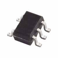
TMP05AKSZ-REEL Analog Devices Inc, TMP05AKSZ-REEL Datasheet - Page 13

TMP05AKSZ-REEL
Manufacturer Part Number
TMP05AKSZ-REEL
Description
IC,TEMPERATURE SENSOR,HYBRID,TSSOP,5PIN,PLASTIC
Manufacturer
Analog Devices Inc
Datasheet
1.TMP05ARTZ-500RL7.pdf
(28 pages)
Specifications of TMP05AKSZ-REEL
Function
Temp Monitoring System (Sensor)
Topology
ADC (Sigma Delta), Averaging Control
Sensor Type
Internal
Sensing Temperature
-40°C ~ 150°C
Output Type
CMOS/TTL
Output Alarm
No
Output Fan
No
Voltage - Supply
3 V ~ 5.5 V
Operating Temperature
-40°C ~ 150°C
Mounting Type
Surface Mount
Package / Case
SC-70-5, SC-88A, SOT-323-5, SOT-353, 5-TSSOP
Lead Free Status / RoHS Status
Lead free / RoHS Compliant
THEORY OF OPERATION
CIRCUIT INFORMATION
The TMP05/TMP06 are monolithic temperature sensors that
generate a modulated serial digital output that varies in direct
proportion with the temperature of each device. An on-board
sensor generates a voltage precisely proportional to absolute
temperature, which is compared to an internal voltage reference
and is input to a precision digital modulator. The ratiometric
encoding format of the serial digital output is independent of
the clock drift errors common to most serial modulation
techniques such as voltage-to-frequency converters. Overall
accuracy for the A grade is ±2°C from 0°C to +70°C with
excellent transducer linearity. B grade accuracy is ±1°C from
0°C to 70°C. The digital output of the TMP05 is CMOS-/TTL-
compatible and is easily interfaced to the serial inputs of most
popular microprocessors. The open-drain output of the TMP06
is capable of sinking 5 mA.
The on-board temperature sensor has excellent accuracy and
linearity over the entire rated temperature range without
correction or calibration by the user.
The sensor output is digitized by a first-order Σ-Δ modulator,
also known as the charge balance type analog-to-digital
converter. This type of converter utilizes time-domain over-
sampling and a high accuracy comparator to deliver 12 bits of
effective accuracy in an extremely compact circuit.
CONVERTER DETAILS
The Σ-Δ modulator consists of an input sampler, a summing
network, an integrator, a comparator, and a 1-bit DAC. Similar
to the voltage-to-frequency converter, this architecture creates,
in effect, a negative feedback loop whose intent is to minimize
the integrator output by changing the duty cycle of the
comparator output in response to input voltage changes. The
comparator samples the output of the integrator at a much
higher rate than the input sampling frequency, which is called
oversampling. Oversampling spreads the quantization noise
over a much wider band than that of the input signal, improving
overall noise performance and increasing accuracy.
VOLTAGE REF
GENERATOR
AND VPTAT
CLOCK
Figure 20. First-Order Σ-∆ Modulator
+
–
INTEGRATOR
Σ-Δ MODULATOR
1-BIT
DAC
COMPARATOR
+
–
DIGITAL
FILTER
TMP05/TMP06
(SINGLE-BIT)
OUT
Rev. B | Page 13 of 28
The modulated output of the comparator is encoded using a
circuit technique that results in a serial digital signal with a
mark-space ratio format. This format is easily decoded by any
microprocessor into either °C or °F values, and is readily
transmitted or modulated over a single wire. More importantly,
this encoding method neatly avoids major error sources
common to other modulation techniques because it is clock-
independent.
FUNCTIONAL DESCRIPTION
The output of the TMP05/TMP06 is a square wave with a
typical period of 116 ms at 25°C (CONV/IN pin is left floating).
The high period, T
with measured temperature. The output format for the nominal
conversion rate is readily decoded by the user as follows:
The time periods T
values easily read by a microprocessor timer/counter port, with
the above calculations performed in software. Because both
periods are obtained consecutively using the same clock,
performing the division indicated in Equation 1 results in a
ratiometric value independent of the exact frequency or drift of
the TMP05/TMP06 originating clock or the user’s counting clock.
OPERATING MODES
The user can program the TMP05/TMP06 to operate in three
different modes by configuring the FUNC pin on power-up as
either low, floating, or high.
Table 6. Operating Modes
FUNC Pin
Low
Floating
High
Continuously Converting Mode
In continuously converting mode, the TMP05/TMP06 continu-
ously output a square wave representing temperature. The
frequency at which this square wave is output is determined by
the state of the CONV/IN pin on power-up. Any change to the
state of the CONV/IN pin after power-up is not reflected in the
parts until the TMP05/TMP06 are powered down and back up.
Temperature (°C) = 421 − (751 × (T
T
H
Figure 21. TMP05/TMP06 Output Format
H
H
, is constant, while the low period, T
(high period) and T
Operating Mode
One shot
Continuously converting
Daisy-chain
H
L
TMP05/TMP06
/T
T
(low period) are
L
L
))
L
, varies
(1)


