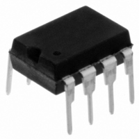
TC1427EPA Microchip Technology, TC1427EPA Datasheet - Page 6

TC1427EPA
Manufacturer Part Number
TC1427EPA
Description
IC,Dual MOSFET Driver,CMOS,DIP,8PIN,PLASTIC
Manufacturer
Microchip Technology
Datasheet
1.TC1427COA713.pdf
(14 pages)
Specifications of TC1427EPA
Configuration
Low-Side
Input Type
Non-Inverting
Delay Time
70ns
Current - Peak
1.2A
Number Of Configurations
2
Number Of Outputs
2
Voltage - Supply
4.5 V ~ 16 V
Operating Temperature
-40°C ~ 85°C
Mounting Type
Through Hole
Package / Case
8-DIP (0.300", 7.62mm)
Lead Free Status / RoHS Status
Lead free / RoHS Compliant
High Side Voltage - Max (bootstrap)
-
Lead Free Status / Rohs Status
Lead free / RoHS Compliant
Available stocks
Company
Part Number
Manufacturer
Quantity
Price
Company:
Part Number:
TC1427EPA
Manufacturer:
Microchip Technology
Quantity:
135
Company:
Part Number:
TC1427EPA
Manufacturer:
MICROCHIP
Quantity:
12 000
Part Number:
TC1427EPA
Manufacturer:
MICROCHIP/微芯
Quantity:
20 000
TC1426/TC1427/TC1428
3.0
3.1
Large currents are required to charge and discharge
capacitive loads quickly. For example, charging a 1000
pF load to 16V in 25 nsec requires a 0.8A current from
the device's power supply.
To ensure low supply impedance over a wide frequency
range, a parallel capacitor combination is recom-
mended for supply bypassing. Low-inductance ceramic
MLC capacitors with short lead lengths (<0.5-in.)
should be used. A 1.0 μF film capacitor in parallel with
one or two 0.1 μF ceramic MLC capacitors normally
provides adequate bypassing.
3.2
The TC1426 and TC1428 contain inverting drivers.
Individual ground returns for the input and output
circuits or a ground plane should be used. This will
reduce negative feedback that causes degradation in
switching speed characteristics.
FIGURE 3-1:
Time
DS21393C-page 6
Test Circuit
Output
Input
V
+5V
0V
DD
0V
Input
APPLICATIONS INFORMATION
SUPPLY BYPASSING
GROUNDING
10%
90%
t
D1
(1/2 TC1428)
10%
V
TC1426
DD
Inverting Driver Switching
t
1
2
F
= 16V
1 μF
WIMA
MKS-2
t
D2
C
L
90%
0.1 μF MLC
Output
= 1000 pF
t
R
10%
90%
3.3
The input voltage level changes the no-load or
quiescent supply current. The N-channel MOSFET
input stage transistor drives a 2.5 mA current source
load. With a logic ‘1’ input, the maximum quiescent
supply current is 9 mA. Logic ‘0’ input level signals
reduce quiescent current to 500 μA maximum. Unused
driver inputs must be connected to V
Minimum power dissipation occurs for logic ‘0’ inputs
for the TC1426/TC1427/TC1428.
The drivers are designed with 100 mV of hysteresis.
This provides clean transitions and minimizes output
stage current spiking when changing states. Input
voltage thresholds are approximately 1.5V, making a
logic ‘1’ input any voltage greater than 1.5V up to V
Input current is less than 1 μA over this range.
The TC1426/TC1427/TC1428 may be directly driven
by the TL494, SG1526/27, TC38C42, TC170 and
similar switch-mode power supply integrated circuits.
FIGURE 3-2:
Switching Time
Test Circuit
Output
Input
V
+5V
DD
0V
0V
INPUT STAGE
Input
10%
t
D1
(1/2 TC1428)
90%
V
Noninverting Driver
TC1427
DD
© 2006 Microchip Technology Inc.
10%
1
2
= 16V
t
R
1 μF
WIMA
MKS-2
t
90%
D2
C
L
0.1 μF MLC
DD
Output
= 1000 pF
10%
or GND.
90%
DD
t
F
.


