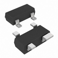
TC1270ASVRCTR Microchip Technology, TC1270ASVRCTR Datasheet - Page 23

TC1270ASVRCTR
Manufacturer Part Number
TC1270ASVRCTR
Description
IC,Power Supply Supervisor,TO-253,4PIN,PLASTIC
Manufacturer
Microchip Technology
Type
Simple Reset/Power-On Resetr
Datasheet
1.TC1270ALVRCTR.pdf
(48 pages)
Specifications of TC1270ASVRCTR
Number Of Voltages Monitored
1
Output
Push-Pull, Totem Pole
Reset
Active Low
Reset Timeout
140 ms Minimum
Voltage - Threshold
2.93V
Operating Temperature
-40°C ~ 125°C
Mounting Type
Surface Mount
Package / Case
SOT-143, SOT-143B, TO-253AA
Lead Free Status / RoHS Status
Lead free / RoHS Compliant
Available stocks
Company
Part Number
Manufacturer
Quantity
Price
Part Number:
TC1270ASVRCTR
Manufacturer:
MIC
Quantity:
20 000
4.3
The minimum pulse width (time) required to cause a
Reset
implementation of a Power-on Reset (POR) circuit.
This time is referred to as transient duration. The
TC127XA devices are designed to reject a level of
negative-going transients (glitches) on the power
supply line.
Transient duration is the amount of time needed for
these supervisory devices to respond to a drop in V
The transient duration time (t
magnitude of V
of duration and overdrive that lies under the duration/
overdrive curve will not generate a Reset signal.
Generally speaking, the transient duration time
decreases with an increase in the V
Figure 4-9
Reset comparator overdrive. It shows that the farther
below the trip point the transient pulse goes, the shorter
the duration of the pulse required to cause a Reset
gets. So, any combination of duration and overdrive
that lays under the curve will not generate a Reset
signal. Combinations above the curve are detected as
a brown-out or power-down.
Transient immunity can be improved by adding a
bypass capacitor (typically 0.1 µF) as close as possible
to the V
FIGURE 4-9:
Transient Duration Waveform.
2010 Microchip Technology Inc.
5V
0V
DD
may
Negative-Going V
Transient Overdrive Voltage (mV)
pin of the TC127XA device.
shows an example transient duration vs.
Area above curve will
generate a Reset signal
TRIP
be
Area below curve will
not generate a Reset signal
– V
an
Time (µs)
Example of Typical
DD
important
(overdrive). Any combination
t
V
(Overdrive)
TRAN
TRAN
TRIP(MIN)
DD
) is dependent on the
(Duration)
TRIP
Transients
criteria
- V
– V
DD
V
V
DD
TRIP(MAX)
TRIP(MIN)
voltage.
in
the
DD
.
4.4
The Manual Reset input pin (MR) allows the Reset pins
(RST/RST) to be manually forced to their active states.
The MR pin has circuitry to filter noise pulses that may
be present on the pin.
diagram for using the TC127XA with a push button
switch. To minimize the required external components,
the MR input has an internal pull-up resistor.
A mechanical push button or active logic signal can
drive the MR input.
Once MR has been low for a time, t
Reset delay time), the Reset output pins are forced
active. The Reset output pins will remain in their active
states for the Reset Delay Timer time out period (t
Figure 4-11
switch input and the Reset pins output.
FIGURE 4-10:
FIGURE 4-11:
4.4.1
The noise filter filters out noise spikes (glitches) on the
Manual Reset pin (MR). Noise spikes less than 100 ns
(typical) are filtered.
MR
RST
RST
The MR input typically ignores input pulses
of 100 ns.
TC1270A/70AN/71A
Manual Reset with Glitch Filter
Circuit
NOISE FILTER
V
shows a waveform for the manual Reset
IL
MR
t
MD
TC127XA
V
+5V
V
DD
t
SS
MR
Push Button Reset.
MR Input – Push Button.
RST
Figure 4-10
V
MCLR
IH
DS22035C-page 23
t
RST
PIC
MD
shows a block
(the manual
®
MCU
RST
).


