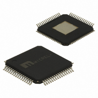
SY89824LHZ Micrel Inc, SY89824LHZ Datasheet - Page 5

SY89824LHZ
Manufacturer Part Number
SY89824LHZ
Description
500MHz 1:22 Diff. HSTL Fanout Buffer ( )
Manufacturer
Micrel Inc
Series
Precision Edge®r
Type
Fanout Buffer (Distribution), Multiplexerr
Datasheet
1.SY89824LHZ.pdf
(7 pages)
Specifications of SY89824LHZ
Number Of Circuits
1
Ratio - Input:output
2:22
Differential - Input:output
Yes/Yes
Input
HSTL, LVPECL
Output
HSTL
Voltage - Supply
3 V ~ 3.6 V
Operating Temperature
0°C ~ 85°C
Mounting Type
Surface Mount
Package / Case
64-TQFP Exposed Pad, 64-eTQFP, 64-HTQFP, 64-VQFP
Lead Free Status / RoHS Status
Lead free / RoHS Compliant
Frequency-max
-
Lead Free Status / RoHS Status
Lead free / RoHS Compliant
Other names
576-2565
SY89824LHZ
SY89824LHZ
Available stocks
Company
Part Number
Manufacturer
Quantity
Price
Company:
Part Number:
SY89824LHZ
Manufacturer:
MICREL
Quantity:
62
Company:
Part Number:
SY89824LHZ
Manufacturer:
MICREL
Quantity:
305
Company:
Part Number:
SY89824LHZTR
Manufacturer:
MICREL
Quantity:
200
Micrel, Inc.
NOTES:
1. Outputs loaded with 50 to ground. Airflow
2. Differential propagation delay is defined as the delay from the crossing point of the differential input signals to the crossing point of the differential
3. The within-device skew is defined as the worst case difference between any two similar delay paths within a single device operating at the same
4. The part-to-part skew is defined as the absolute worst case difference between any two delay paths on any two devices operating at the same
5. The V
6. V
7. OE set-up time is defined with respect to the rising edge of the clock. OE HIGH to LOW transition ensures outputs remain disabled during the next
M9999-020207
hbwhelp@micrel.com or (408) 955-1690
Symbol
t
t
t
V
V
t
t
t
tf
PD
SKEW
SKPP
S
H
r
AC ELECTRICAL CHARACTERISTICS
PP
CMR
output signals.
voltage and temperature.
voltage and temperature.
the table are referenced to V
The lower end of the CMR range varies 1:1 with V
clock cycle. OE LOW to HIGH transition enables normal operation of the next input clock.
CMR
PP
is defined as the range within which the V
(min.) is defined as the minimum input differential voltage which will cause no increase in the propagation delay.
Propagation Delay
Within-Device Skew
Part-to-Part Skew
Minimum Input Swing
LVPECL_CLK
Common Mode Range
LVPECL_CLK
OE Set-Up Time
OE Hold Time
Output Rise/Fall Time
(20% – 80%)
Parameter
CCI
(7)
(4)
. The V
(2)
(3)
(5)
(6)
IL
level must be such that the peak-to-peak voltage is less than 1.0V and greater than or equal to V
300lfpm.
IH
CCI
level may vary, with the device still meeting the propagation delay specification. The numbers in
Min.
–1.5
600
300
1.0
0.5
—
—
—
. The V
T
CMR
(1)
A
Typ.
= 0 C
1.0
—
—
—
—
—
—
—
(min) will be fixed at 3.3V – |V
Max.
–0.4
5
200
700
50
—
—
—
—
Min.
–1.5
600
300
1.0
0.5
—
—
—
T
A
= +25 C
Typ.
1.0
—
—
—
—
—
—
—
CMR
(min)|.
Max.
–0.4
200
700
50
—
—
—
—
Min.
–1.5
600
300
1.0
0.5
—
—
—
T
A
= +85 C
Typ.
1.0
—
—
—
—
—
—
—
Precision Edge
Max.
–0.4
200
700
50
—
—
—
—
SY89824L
PP
(min.).
Unit
mV
ns
ps
ps
ns
ns
ps
V
®


