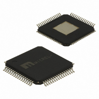
SY87725LHY TR Micrel Inc, SY87725LHY TR Datasheet - Page 4

SY87725LHY TR
Manufacturer Part Number
SY87725LHY TR
Description
3.3V ONU SERDES (I Temp, /60 Pin EP-TQFP/T+R)
Manufacturer
Micrel Inc
Type
Transceiverr
Datasheet
1.SY87725LHY.pdf
(20 pages)
Specifications of SY87725LHY TR
Protocol
LVDS
Voltage - Supply
3.15 V ~ 3.45 V
Mounting Type
Surface Mount
Package / Case
64-TQFP Exposed Pad, 64-eTQFP, 64-HTQFP, 64-VQFP
Lead Free Status / RoHS Status
Lead free / RoHS Compliant
Number Of Drivers/receivers
-
Lead Free Status / RoHS Status
Lead free / RoHS Compliant
Other names
SY87725LHYTR
SY87725LHYTR
SY87725LHYTR
Pin Description
July 2007
RECEIVE SECTION SIGNALS
Pin Number
TRANSMIT SECTION SIGNALS
25, 26, 27,
28, 29, 30,
39, 40,
41, 42,
43, 44,
55, 56
60, 61
45, 46
33, 34
36, 37
31, 32
22, 23
10, 14
11, 12
49, 50
6, 7
1, 2
3, 5
15
59
18
63
62
24
DOUTOP, DOUT0N,
DOUT1P, DOUT1N,
DOUT2P, DOUT2N,
DOUT3P, DOUT3N
CLKINP, CLKINN
SOUTP, SOUTN
DIN0P, DIN0N,
DIN1P, DIN1N,
DIN2P, DIN2N,
REFFREQSEL
RCV_DDRSEL
XMT_DDRSEL
DIN3P, DIN3N
RCV_PLLRP,
RCV_PLLSN,
XMT_PLLSN,
RCV_FSEL0,
XMT_FSEL0,
RCV_PLLRN
RCV_PLLSP
XMT_PLLSP
RCV_FSEL1
XMT_FSEL1
CLKOUT2P,
RCV_SYNC
SINP, SINN
CLKOUT2N
CLKOUTP,
REFCLKP,
REFCLKN,
CLKOUTN
Pin Name
LFIN
CD
Serial Data In (Differential LVPECL Input): This input receives the serial differential
data stream. An internal PLL recovers the embedded clock and data.
Reference Clock (TTL or Differential LVPECL Input): This input accepts either single-
ended TTL or differential LVPECL signals and is used as the reference for the internal
frequency synthesizer and the “training” frequency for the receiver PLL to keep it
centered in the absence of data at the SIN input. The REFCLKN input has an internal
reference circuit that applies the threshold voltage in case of a single-ended TTL-
signal at REFCLKP. REFCLKN has an internal 75kΩ to GND and
in that case.
Reference Clock Frequency Select (TTL Input): Selects REFCLK frequency of
77.76MHz when LOW or 155.52MHz when HIGH.
Clock Recovery PLL Loop Filter: External loop filter pins for the receive PLL.
Clock Synthesis PLL Loop Filter: External loop filter pins for the clock synthesis PLL.
Receive Synchronizer (TTL Input): Single-ended asynchronous input to set the word
boundary on the 4-bit parallel data
Receive Frequency Control (TTL Inputs): Two single-ended frequency selects for
receive synthesizer.
Parallel Data Out (LVDS Outputs): These are the four pairs of receive parallel data
outputs.
Parallel Clock Out (LVDS Output): This output is the recovered clock at the transmit
byte clock rate and provides a clock that can be used as a reference clock to drive
CLKIN.
Parallel Clock Out (LVDS Output): This output is the recovered clock divided by 4 or 8
to provide the parallel data rate clock.
Link Fault Indicator (TTL Output): When HIGH, LFIN indicates CDR is “in-lock” and
when LOW it indicates CDR loss-of-lock.
Double Data Rate Select (TTL Input): Selects either parallel data rate clock for normal
operation or one-half of parallel data rate clock for double data rate applications.
Carrier Detect Input (LVPECL input): When HIGH, CD indicates the carrier is present
and when LOW it indicates the loss of carrier.
Parallel Data In (LVDS Inputs): These are the four pairs of transmit parallel data
inputs. Each Differential pair has a 100Ω internal termination across the pair.
Parallel Clock In (LVDS Input): This input is the transmit parallel (byte-rate) clock.
Transmit Frequency Control (TTL Inputs): Two single-ended frequency selects for
transmit synthesizer.
Clock Synthesis PLL Loop Filter: External loop filter pins for the clock synthesis PLL.
Serial Data Out (Differential CML Output): This is the serial differential data stream
output.
Double Data Rate Select (TTL Input): Selects either parallel data rate clock for normal
operation or one-half of parallel data rate clock for double data rate applications.
4
Pin Description
hbwhelp@micrel.com
can be left open
or (408) 955-1690
M9999-071007-B


