SY58611UMG TR Micrel Inc, SY58611UMG TR Datasheet
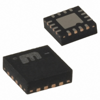
3.2Gbps 2:1 LVDS Mux W/ FSI Inputs

SY58611UMG TR

Manufacturer Part Number
SY58611UMG TR
Description
3.2Gbps 2:1 LVDS Mux W/ FSI Inputs
Manufacturer
Micrel Inc
Series
SY58r
Type
Multiplexerr
Datasheet

Specifications of SY58611UMG TR

Circuit
2 x 2:1
Independent Circuits
1
Voltage Supply Source
Single Supply
Voltage - Supply
3 V ~ 3.6 V
Operating Temperature
-40°C ~ 85°C
Mounting Type
Surface Mount
Package / Case
16-MLF®, QFN
Number Of Elements
1
Number Of Receivers
2
Number Of Drivers
1
Input Type
CMOS/TTL
Operating Supply Voltage (typ)
2.5V
Transmission Data Rate
3200Mbps
Propagation Delay Time
0.47ns
Operating Temp Range
-40C to 85C
Operating Temperature Classification
Industrial
Mounting
Surface Mount
Pin Count
16
Lead Free Status / RoHS Status
Lead free / RoHS Compliant
Current - Output High, Low
-
Lead Free Status / Rohs Status
Compliant
Other names
SY58611UMGTR
SY58611UMGTR
General Description
The SY58611U is a 2.5V, high-speed, fully differential
LVDS 2:1 MUX capable of processing clocks up to
2.5GHz and data up to 3.2Gbps. SY58611U is
optimized to provide a buffered output of the selected
input with less than 20ps of skew and less than 10ps
total jitter. Patented MUX Isolation design reduces
crosstalk and provides superior signal integrity.
The differential inputs include Micrel’s unique, 3-pin
input termination architecture that interfaces to LVPECL,
LVDS or CML differential signals, (AC- or DC-coupled)
as small as 100mV
shifting or termination resistor networks in the signal
path. For AC-coupled input interface applications, an
integrated reference voltage (V
the V
times guaranteed to be less than 120ps.
The SY58611U operates from a 2.5V ±5% supply and is
guaranteed over the full industrial temperature range
(–40°C to +85°C). For applications that require CML or
LVPECL output, consider the SY58609U and
SY58610U, 2:1 MUX with 400mV and 800mV output
swings respectively. The SY58611U is part of Micrel’s
high-speed, Precision Edge
Datasheets and support documentation can be found on
Micrel’s web site at: www.micrel.com.
Functional Block Diagram
March 2007
Precision Edge is a registered trademark of Micrel, Inc.
T
Micrel Inc. • 2180 Fortune Drive • San Jose, CA 95131 • USA • tel +1 (408) 944-0800 • fax + 1 (408) 474-1000 • http://www.micrel.com
pin. The output is LVDS compatible, with rise/fall
PK
(200mV
®
product line.
REF-AC
pp
) without any level-
) is provided to bias
pp
Features
∑ Selects between two sources and provides buffered
∑ Fail Safe Input
∑ Guaranteed AC performance over temperature and
∑ Unique, patented internal termination and VT pin
∑ Unique, patented MUX input isolation design
∑ Ultra-low jitter design
∑ 2.5V ±5% power supply operation
∑ Industrial temperature range: –40°C to +85°C
∑ Available in 16-pin (3mm x 3mm) QFN package
Applications
∑ All SONET clock distribution
∑ Fibre Channel clock and data distribution
∑ Gigabit Ethernet clock or data distribution
∑ Backplane distribution
Markets
∑ DataCom and Telecom
∑ Storage
∑ ATE
∑ Test and Measurement
Internal Termination and Fail Safe Input
3.2Gbps Precision, LVDS 2:1 MUX with
copy of the selected input signal
– Prevents output from oscillating when input is
voltage:
– DC-to > 3.2Gbps throughput
– <420ps typical propagation delay (IN-to-Q)
– <120ps rise/fall times
accepts DC- and AC-coupled inputs (CML, PECL,
LVDS)
minimizes adjacent channel crosstalk
– <1ps
– <10ps
– <1ps
– <10ps
invalid or removed
RMS
RMS
PP
PP
total jitter
deterministic jitter
cycle-to-cycle jitter
random jitter
SY58611U
hbwhelp@micrel.com
or (408) 955-1690
Precision Edge
M9999-030607-A
®

Related parts for SY58611UMG TR

SY58611UMG TR Summary of contents

Page 1

... Functional Block Diagram Precision Edge is a registered trademark of Micrel, Inc. Micrel Inc. • 2180 Fortune Drive • San Jose, CA 95131 • USA • tel +1 (408) 944-0800 • fax + 1 (408) 474-1000 • http://www.micrel.com March 2007 3.2Gbps Precision, LVDS 2:1 MUX with ...

Page 2

Ordering Information Part Number Package SY58611UMG QFN-16 (2) SY58611UMGTR QFN-16 Notes: 1. Contact factory for die availability. Dice are guaranteed Tape and Reel. Pin Configuration 16-Pin QFN Pin Description Pin Number Pin Name Pin Function 1, ...

Page 3

Absolute Maximum Ratings Supply Voltage (V ) ................................. –0.5V to +4.0V CC Input Voltage (V ) ......................................... –0. LVDS Output Current (I ) ................................... ±10mA OUT Input Current Source or Sink Current on (IN, /IN)................. ±50mA Current ...

Page 4

LVDS Output DC Electrical Characteristics V = +2.5V ±5 100Ω across the output pair Symbol Parameter V Output Voltage Swing (Q, /Q) OUT V Differential Output Voltage Swing |Q-/Q| DIFF_OUT V Output Common Mode Voltage ...

Page 5

AC Electrical Characteristics V = +2.5V ±5 100Ω across the output pair; Input Symbol Parameter f Maximum Frequency MAX t Propagation Delay PD SEL-to-Q t Input-to-Input Skew Skew Part-to-Part Skew t Data Random Jitter Jitter ...

Page 6

Functional Description Fail-Safe Input (FSI) The input includes a special fail-safe circuit to sense the amplitude of the input signal and to latch the output when there is no input signal present, or when the amplitude of the input signal ...

Page 7

Input Stage Single-Ended and Differential Swings Figure 3a. Single-Ended Swing March 2007 Figure 1c. SEL-to-Q Delay Figure 2. Simplified Differential Input Buffer 7 Figure 3b. Differential Swing M9999-030607-A hbwhelp@micrel.com or (408) 955-1690 ...

Page 8

Typical Characteristics V = 2.5V, GND = 0V 100mV March 2007 = 100Ω across the output pair 25°C, unless otherwise stated. A M9999-030607-A hbwhelp@micrel.com or (408) 955-1690 ...

Page 9

Functional Characteristics V = 2.5V, GND = 0V 325mV March 2007 = 100Ω across the output pair 25°C, unless otherwise stated. A M9999-030607-A hbwhelp@micrel.com or (408) 955-1690 ...

Page 10

Functional Characteristics V = 2.5V, GND = 0V 325mV March 2007 (continued) = 100Ω across the output pair 25°C, unless otherwise stated. A M9999-030607-A hbwhelp@micrel.com or (408) 955-1690 ...

Page 11

Input Interface Applications Figure 4a. CML Interface (DC-Coupled) Option: May connect V to VCC T Figure 4d. LVPECL Interface (AC-Coupled) March 2007 Figure 4b. CML Interface (AC-Coupled) Figure 4e. LVDS Interface 11 Figure 4c. LVPECL Interface (DC-Coupled) M9999-030607-A hbwhelp@micrel.com or ...

Page 12

LVDS Output Interface Applications LVDS specifies a small swing of 325mV typical nominal 1.2V common mode above ground. The common mode voltage has tight limits to permit large variations in the ground between and LVDS driver and receiver. ...

Page 13

Package Information MICREL, INC. 2180 FORTUNE DRIVE SAN JOSE, CA 95131 USA TEL +1 (408) 944-0800 FAX +1 (408) 474-1000 WEB http:/www.micrel.com The information furnished by Micrel in this data sheet is believed to be accurate and reliable. However, no ...

Related keywords