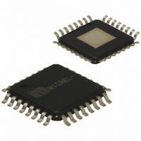
SY55856UHG TR Micrel Inc, SY55856UHG TR Datasheet - Page 7

SY55856UHG TR
Manufacturer Part Number
SY55856UHG TR
Description
2.5V/3.3V 2.5GHz 2 Channel Delay Line (I Temp, Green)
Manufacturer
Micrel Inc
Datasheet
1.SY55856UHG.pdf
(9 pages)
Specifications of SY55856UHG TR
Function
Delay Generator
Delay To 1st Tap
50pS
Tap Increment
50ps
Available Total Delays
.35ns
Number Of Independent Delays
7
Voltage - Supply
2.3 V ~ 3.6 V
Operating Temperature
-40°C ~ 85°C
Mounting Type
Surface Mount
Package / Case
32-TQFP Exposed Pad, 32-eTQFP, 32-HTQFP, 32-VQFP
Lead Free Status / RoHS Status
Lead free / RoHS Compliant
Number Of Taps/steps
-
Lead Free Status / Rohs Status
Compliant
Other names
SY55856UHGTR
SY55856UHGTR
SY55856UHGTR
Micrel, Inc.
V
Note 1.
Note 2.
Note 3.
Note 4.
Note 5.
V
Note 6.
M9999-021908
hbwhelp@micrel.com or (408) 955-1690
Symbol
V
I
CC
Symbol
V
V
V
V
CC
V
Symbol
V
V
V
V
V
V
(Swing)
R
CC
DC ELECTRICAL CHARACTERISTICS
CC
VT INPUTS DC ELECTRICAL CHARACTERISTICS
ILVL
IHVT
ILVT
TCL
CML DC ELECTRICAL CHARACTERISTICS
IST
ID
IH
IL
OH
OL
OUT
OUT
= 2.3V to 3.6V; GND = 0V; T
= 2.3V to 3.6V; GND = 0V; T
DC parameters are guaranteed after thermal equilibrium has been established.
The LVL input determines the voltage switching threshold that differentiates logic high from logic low for the V
DELAY_SEL, and CINV. LVL may be driven to V
logic high. Also, as shown in Figure 3, the LVL input internally clamps at V
maximum of
V
V
between V
V
V
V
immunity purposes is 2 × V
400mV swing is available in a 50Ω environment. Refer to “CML Termination” figures for more details.
V
T
SW
IST
IST
OUT(SWING)
CC
inputs are S0, S1, S2, DELAY_SEL, and CINV.
Differential Input Voltage
Input HIGH Voltage
Input LOW Voltage
Output HIGH Voltage
Output LOW Voltage
Output Voltage Swing
Output Source Impedance
(CLK_OUT, /CLK_OUT and
DATA_OUT, /DATA_OUT)
Power Supply Voltage
Power Supply Current
Analog Input
V
V
Input Switching Threshold
Differential Voltage
Threshold Clamp Voltage
+
is the voltage difference needed to guarantee a stable logic level. Logic high must be at least V
below V
is the threshold switching voltage. It is equal to the voltage at the LVL pin, when this voltage is above V
2
T
T
GND
Input High Voltage
Input High Voltage
TCL
Parameter
Parameter
Parameter
SW
=
is defined as the swing on one output of a differential pair, that is |V
(min) and V
V
. Thus, the minimum input swing on a given V
CC
2
(2)
and V
(5)
TCL
TCL
OUT(SWING)
(6)
(3,4)
(3,4)
.
(max) when the Voltage at the LVL pin is below V
A
A
= –40°C to +85°C
= –40°C to +85°C
Min.
. Actual voltage levels and differential swing will depend on customer termination scheme. Typically, a
2.3
—
V
V
T
CC
V
CC
A
0.650
SW
Min.
100
= –40
1.6
1.5
Typ.
V
Min.
–0.040
—
40
100
0.0
1.2
–1.00
—
—
TCL
CC
+ 0.1
, but this is not useful, as the V
°
C
(1)
Max.
140
3.6
T
input pin, that is, |V
7
Min.
2.3
—
V
V
T
CC
CC
A
0.800
0.400
Typ.
TCL
50
—
—
—
–0.010
–0.800
= +25
Typ.
Typ.
115
50
—
—
—
—
—
. If LVL is left unconnected, the V
TCL
OH
°
C
T
IHVT
(max).
- V
Max.
inputs could then not get high enough to reliably indicate
140
3.6
OL
- V
| on one pin. The swing for common mode noise
ILVT
Min.
|, must be at least 2×V
2.3
—
V
T
IST
V
V
V
CC
A
IH
SW
Max.
1.00
CC
V
V
= +85
Max.
above V
Typ.
—
—
60
V
1.4
CC
CC
–0.65
–0.1
—
—
—
CC
– 0.1
- 0.1
TCL
T
°
C
T
inputs S0, S1, S2,
SW
(max). V
Max.
inputs will switch at about the
140
3.6
. Logic low must be at most
IST
Unit
.
mV
SW
Ω
V
V
V
V
V
Unit
mA
V
is some value
50Ω Environment
Condition
SuperLite™
Unit
Condition
No Load
No Load
No Load
mV
SY55856U
No Load
V
V
V
V


