SSM2356CBZ-RL Analog Devices Inc, SSM2356CBZ-RL Datasheet - Page 14
SSM2356CBZ-RL
Manufacturer Part Number
SSM2356CBZ-RL
Description
2x2W Filterless Class D Stereo Audio Amp
Manufacturer
Analog Devices Inc
Type
Class Dr
Datasheet
1.SSM2356CBZ-RL.pdf
(16 pages)
Specifications of SSM2356CBZ-RL
Output Type
2-Channel (Stereo)
Max Output Power X Channels @ Load
2.5W x 2 @ 4 Ohm
Voltage - Supply
2.5 V ~ 5.5 V
Features
Depop, Differential Inputs, Short-Circuit and Thermal Protection, Shutdown
Mounting Type
Surface Mount
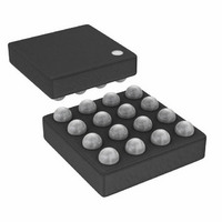
Package / Case
16-WLCSP
Lead Free Status / RoHS Status
Lead free / RoHS Compliant


SSM2356
The measurements for Figure 36 and Figure 37 were taken in
an FCC-certified EMI laboratory with a 1 kHz input signal,
producing 0.5 W output power into an 8 Ω load from a 5 V
supply. Cable length was 12 cm, unshielded twisted pair
speaker cable. Note that reducing the supply voltage greatly
reduces radiated emissions.
OUTPUT MODULATION DESCRIPTION
The SSM2356 uses three-level, Σ-Δ output modulation. Each
output can swing from GND to V
no input signal is present, the output differential voltage is 0 V
because there is no need to generate a pulse. In a real-world
situation, there are always noise sources present.
Due to this constant presence of noise, a differential pulse is
generated, when required, in response to this stimulus. A small
amount of current flows into the inductive load when the differ-
ential pulse is generated. However, most of the time, output
differential voltage is 0 V, due to the Analog Devices three-level,
Σ-Δ output modulation. This feature ensures that the current
flowing through the inductive load is small.
When the user wants to send an input signal, an output pulse is
generated to follow input voltage. The differential pulse density
is increased by raising the input signal level. Figure 38 depicts
three-level, Σ-Δ output modulation with and without input
stimulus.
LAYOUT
As output power continues to increase, care must be taken to
lay out PCB traces and wires properly among the amplifier,
load, and power supply. A good practice is to use short, wide
PCB tracks to decrease voltage drops and minimize inductance.
Ensure that track widths are at least 200 mil for every inch of
track length for the lowest dc resistance (DCR), and use 1 oz. or
2 oz. copper PCB traces to further reduce IR drops and
inductance. A poor layout increases voltage drops, consequently
VOUT
VOUT
VOUT
OUT+
OUT–
OUT+
OUT–
OUT+
OUT–
OUTPUT = 0V
OUTPUT > 0V
OUTPUT < 0V
Figure 38. Three-Level, Σ-Δ Output Modulation With and
Without Input Stimulus
DD
and vice versa. Ideally, when
+5V
0V
+5V
0V
+5V
0V
–5V
+5V
0V
+5V
0V
+5V
0V
+5V
0V
+5V
0V
0V
–5V
Rev. 0 | Page 14 of 16
affecting efficiency. Use large traces for the power supply inputs
and amplifier outputs to minimize losses due to parasitic trace
resistance. Proper grounding guidelines help to improve audio
performance, minimize crosstalk between channels, and prevent
switching noise from coupling into the audio signal.
To maintain high output swing and high peak output power, the
PCB traces that connect the output pins to the load and supply
pins should be as wide as possible to maintain the minimum
trace resistances. It is also recommended that a large ground
plane be used for minimum impedances. In addition, good PCB
layout isolates critical analog paths from sources of high inter-
ference. High frequency circuits (analog and digital) should be
separated from low frequency circuits.
Properly designed multilayer PCBs can reduce EMI emission
and increase immunity to the RF field by a factor of 10 or more,
compared with double-sided boards. A multilayer board allows
a complete layer to be used for the ground plane, whereas the
ground plane side of a double-sided board is often disrupted by
signal crossover.
If the system has separate analog and digital ground and power
planes, the analog ground plane should be directly beneath the
analog power plane, and, similarly, the digital ground plane should
be directly beneath the digital power plane. There should be no
overlap between analog and digital ground planes or between
analog and digital power planes.
INPUT CAPACITOR SELECTION
The SSM2356 does not require input coupling capacitors if the
input signal is biased from 1.0 V to VDD − 1.0 V. Input capacitors
are required if the input signal is not biased within this recom-
mended input dc common-mode voltage range, if high-pass
filtering is needed, or if a single-ended source is used. If high-
pass filtering is needed at the input, the input capacitor and the
input resistor of the SSM2356 form a high-pass filter whose
corner frequency is determined by the following equation:
The input capacitor can significantly affect the performance of
the circuit. Not using input capacitors degrades both the output
offset of the amplifier and the dc PSRR performance.
PROPER POWER SUPPLY DECOUPLING
To ensure high efficiency, low total harmonic distortion (THD),
and high PSRR, proper power supply decoupling is necessary.
Noise transients on the power supply lines are short-duration
voltage spikes. These spikes can contain frequency components
that extend into the hundreds of megahertz. The power supply
input must be decoupled with a good quality, low ESL, low ESR
capacitor, greater than 4.7 μF. This capacitor bypasses low freq-
uency noises to the ground plane. For high frequency transient
noises, use a 0.1 μF capacitor as close as possible to the VDD
pin of the device. Placing the decoupling capacitor as close as
possible to the SSM2356 helps to maintain efficient
performance.
f
C
= 1/(2π × R
IN
× C
IN
)
Related parts for SSM2356CBZ-RL
Image
Part Number
Description
Manufacturer
Datasheet
Request
R

Part Number:
Description:
±1.7g Dual-Axis IMEMS Accelerometer Evaluation Board
Manufacturer:
Analog Devices Inc
Datasheet:

Part Number:
Description:
Inertial Sensor Evaluation System
Manufacturer:
Analog Devices Inc
Datasheet:
Part Number:
Description:
Manufacturer:
Analog Devices Inc
Datasheet:
Part Number:
Description:
Manufacturer:
Analog Devices Inc
Datasheet:
Part Number:
Description:
Manufacturer:
Analog Devices Inc
Datasheet:
Part Number:
Description:
Manufacturer:
Analog Devices Inc
Datasheet:
Part Number:
Description:
Manufacturer:
Analog Devices Inc
Datasheet:
Part Number:
Description:
Manufacturer:
Analog Devices Inc
Datasheet:
Part Number:
Description:
Manufacturer:
Analog Devices Inc
Datasheet:
Part Number:
Description:
Manufacturer:
Analog Devices Inc
Datasheet:
Part Number:
Description:
Manufacturer:
Analog Devices Inc
Datasheet:
Part Number:
Description:
Manufacturer:
Analog Devices Inc
Datasheet:
Part Number:
Description:
Manufacturer:
Analog Devices Inc
Datasheet: