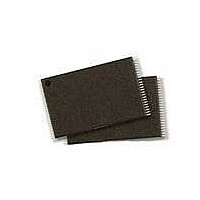
S29JL032H70TFI420 Spansion Inc., S29JL032H70TFI420 Datasheet - Page 32

S29JL032H70TFI420
Manufacturer Part Number
S29JL032H70TFI420
Description
IC,EEPROM,NOR FLASH,2MX16/4MX8,CMOS,TSSOP,48PIN,PLASTIC
Manufacturer
Spansion Inc.
Datasheets
1.S29JL032H70TFI420.pdf
(60 pages)
2.S29JL032H70TFI020.pdf
(64 pages)
3.S29JL032H70TFI420.pdf
(66 pages)
Specifications of S29JL032H70TFI420
Data Bus Width
8 bit, 16 bit
Architecture
Boot Sector
Interface Type
Conventional
Access Time
70 ns
Supply Voltage (max)
3.6 V
Supply Voltage (min)
2.7 V
Maximum Operating Current
2 mA
Mounting Style
SMD/SMT
Memory Type
Flash
Memory Size
32 Mbit
Operating Temperature
+ 85 C
Package / Case
TSOP-48
Lead Free Status / RoHS Status
Lead free / RoHS Compliant
Lead Free Status / RoHS Status
Lead free / RoHS Compliant
Available stocks
Company
Part Number
Manufacturer
Quantity
Price
Company:
Part Number:
S29JL032H70TFI420
Manufacturer:
Spansion
Quantity:
2 356
32
Autoselect Command Sequence
Enter SecSi™ Sector/Exit SecSi Sector
Command Sequence
Byte/Word Program Command Sequence
If DQ5 goes high during a program or erase operation, writing the reset command
returns the banks to the read mode (or erase-suspend-read mode if that bank
was in Erase Suspend).
The autoselect command sequence allows the host system to access the manu-
facturer and device codes, and determine whether or not a sector is protected.
The autoselect command sequence may be written to an address within a bank
that is either in the read or erase-suspend-read mode. The autoselect command
may not be written while the device is actively programming or erasing in another
bank.
The autoselect command sequence is initiated by first writing two unlock cycles.
This is followed by a third write cycle that contains the bank address and the au-
toselect command. The bank then enters the autoselect mode. The system may
read any number of autoselect codes without reinitiating the command sequence.
Table
tion information, the system must write to the appropriate bank address (BA) and
sector address (SA). Tables
associated with each sector.
The system must write the reset command to return to the read mode (or erase-
suspend-read mode if the bank was previously in Erase Suspend).
The SecSi Sector region provides a secured data area containing a random, six-
teen-byte electronic serial number (ESN). The system can access the SecSi
Sector region by issuing the three-cycle Enter SecSi Sector command sequence.
The device continues to access the SecSi Sector region until the system issues
the four-cycle Exit SecSi Sector command sequence. The Exit SecSi Sector com-
mand sequence returns the device to normal operation. The SecSi Sector is not
accessible when the device is executing an Embedded Program or embedded
Erase algorithm. Table
m a n d s e q u e n c e s . S e e a l s o “ S e c S i ™ ( S e c u r e d S i l i c o n ) S e c t o r
Flash Memory Region” for further information. Note that the ACC function and un-
lock bypass modes are not available when the SecSi Sector is enabled.
The system may program the device by word or byte, depending on the state of
the BYTE# pin. Programming is a four-bus-cycle operation. The program com-
mand sequence is initiated by writing two unlock write cycles, followed by the
program set-up command. The program address and data are written next, which
in turn initiate the Embedded Program algorithm. The system is not required to
provide further controls or timings. The device automatically provides internally
generated program pulses and verifies the programmed cell margin. Table
shows the address and data requirements for the byte program command
sequence.
When the Embedded Program algorithm is complete, that bank then returns to
the read mode and addresses are no longer latched. The system can determine
the status of the program operation by using DQ7, DQ6, or RY/BY#. Refer to the
Write Operation Status section for information on these status bits.
13
shows the address and data requirements. To determine sector protec-
13
shows the address and data requirements for both com-
A D V A N C E
3
and
4
S29JL032H
show the address range and bank number
I N F O R M A T I O N
13
S29JL032HA0 May 21, 2004


