PIC16LF1903T-I/SO Microchip Technology, PIC16LF1903T-I/SO Datasheet - Page 212
PIC16LF1903T-I/SO
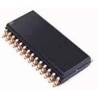
Manufacturer Part Number
PIC16LF1903T-I/SO
Description
7KB Flash, 256B RAM, LCD, 11x10b ADC, NanoWatt XLP 28 SOIC .300in T/R
Manufacturer
Microchip Technology
Series
PIC® XLP™ 16Fr
Datasheet
1.PIC16LF1902-EMV.pdf
(240 pages)
Specifications of PIC16LF1903T-I/SO
Processor Series
PIC16LF190x
Core
PIC
Data Bus Width
8 bit
Program Memory Type
Flash
Program Memory Size
4 KB
Data Ram Size
256 B
Maximum Clock Frequency
20 MHz
Number Of Programmable I/os
25
Number Of Timers
2
Operating Supply Voltage
1.8 V to 3.6 V
Maximum Operating Temperature
+ 85 C
Mounting Style
SMD/SMT
Package / Case
SOIC-28
Core Processor
PIC
Core Size
8-Bit
Speed
20MHz
Connectivity
-
Peripherals
Brown-out Detect/Reset, LCD, POR, PWM, WDT
Number Of I /o
25
Eeprom Size
-
Ram Size
256 x 8
Voltage - Supply (vcc/vdd)
1.8 V ~ 3.6 V
Data Converters
A/D 11x10b
Oscillator Type
Internal
Operating Temperature
-40°C ~ 85°C
Lead Free Status / Rohs Status
Details


PIC16LF1902/3
TABLE 21-6:
TABLE 21-7:
DS41455B-page 212
Standard Operating Conditions (unless otherwise stated)
Operating temperature
AD01
AD02
AD03
AD04
AD05
AD06
AD07
AD08
AD08A
AD09
AD10
AD11
Note 1:
Standard Operating Conditions (unless otherwise stated)
Operating temperature
AD130* T
AD131
AD132* T
AD134
Note 1: The ADRES register may be read on the following T
Param
Param
No.
No.
*
†
*
†
2:
3:
4:
5:
N
E
E
E
E
E
E
V
V
Z
I
Sym.
REF
T
T
AIN
AIN
IL
DL
OFF
GN
ABS
LIN
REF
R
These parameters are characterized but not tested.
Data in “Typ” column is at 3.0V, 25°C unless otherwise stated. These parameters are for design guidance only and are not
tested.
These parameters are characterized but not tested.
Data in “Typ” column is at 3.0V, 25°C unless otherwise stated. These parameters are for design guidance only and are not
tested.
Sym.
AD
CNV
ACQ
GO
Total Absolute Error includes integral, differential, offset and gain errors.
The A/D conversion result never decreases with an increase in the input voltage and has no missing codes.
ADC V
When ADC is off, it will not consume any current other than leakage current. The power-down current specification
includes any such leakage from the ADC module.
Not targeting 1.8V as minimum voltage for die size reasons.
Resolution
Integral Error
Differential Error
Offset Error
Gain Error
Absolute Error
Linearity Error
Reference Voltage
Full-Scale Range
Recommended Impedance of
Analog Voltage Source
V
REF
A/D Clock Period
A/D Internal RC Oscillator
Period
Conversion Time (not including
Acquisition Time)
Acquisition Time
Q4 to A/D Clock Start
Acquisition Time
REF
PIC16LF1902/3 A/D CONVERTER (ADC) CHARACTERISTICS:
PIC16LF1902/3 A/D CONVERSION REQUIREMENTS
Input Current
is from the V
Characteristic
-40°C T
-40°C T
Characteristic
(3)
(3)
(1)
A
A
DD
+125°C
+125°C
pin.
Min.
V
Min.
1.8
2.0
1.6
3.0
3.0
1.6
—
—
—
—
—
—
—
—
10
—
—
—
—
SS
Preliminary
T
Typ†
OSC
—
—
—
—
—
—
—
—
—
—
—
—
—
CY
T
Typ†
OSC
11.5
6.0
4.0
11
—
—
/2+T
cycle.
/2
CY
Max.
V
1000
V
V
10
±1
±1
±1
±1
±1
50
10
±1
REF
DD
DD
Max.
9.0
9.0
9.0
6.0
—
—
—
—
Units
LSb V
LSb No missing codes, V
LSb V
LSb V
LSb V
LSb V
k
A
A
bit
V
V
V
Units
T
Absolute minimum to ensure 1 LSb accuracy
( Note 5 )
Can go higher if external 0.01
present on input pin.
During V
Based on differential of V
During A/D conversion cycle.
s
s
s
s
s
—
—
AD
REF
REF
REF
REF
REF
= 5.0V
= 5.0V
= 5.0V
= 5.0V
= 5.0V
T
T
ADCS<1:0> = 11 (ADRC mode)
at V
at V
Set GO/DONE bit to conversion
complete.
If the A/D clock source is selected as RC,
a time of T
clock starts. This allows the SLEEP
instruction to be executed.
OSC
OSC
AIN
DD
DD
-based, V
-based, V
acquisition.
= 2.0V
= 3.0V
2011 Microchip Technology Inc.
CY
Conditions
is added before the A/D
REF
REF
REF
Conditions
= 5.0V
3.0V
full range
HOLD
to V
F capacitor is
AIN
.
Related parts for PIC16LF1903T-I/SO
Image
Part Number
Description
Manufacturer
Datasheet
Request
R

Part Number:
Description:
IC, 8BIT MCU, PIC16LF, 32MHZ, QFN-28
Manufacturer:
Microchip Technology
Datasheet:

Part Number:
Description:
IC, 8BIT MCU, PIC16LF, 32MHZ, QFN-28
Manufacturer:
Microchip Technology
Datasheet:

Part Number:
Description:
IC, 8BIT MCU, PIC16LF, 32MHZ, DIP-18
Manufacturer:
Microchip Technology
Datasheet:

Part Number:
Description:
IC, 8BIT MCU, PIC16LF, 20MHZ, TQFP-44
Manufacturer:
Microchip Technology
Datasheet:
Part Number:
Description:
7 KB Flash, 384 Bytes RAM, 32 MHz Int. Osc, 16 I/0, Enhanced Mid Range Core, Nan
Manufacturer:
Microchip Technology

Part Number:
Description:
14KB Flash, 512B RAM, LCD, 11x10b ADC, EUSART, NanoWatt XLP 28 SOIC .300in T/R
Manufacturer:
Microchip Technology
Datasheet:
Part Number:
Description:
14KB Flash, 512B RAM, LCD, 11x10b ADC, EUSART, NanoWatt XLP 28 SSOP .209in T/R
Manufacturer:
Microchip Technology
Datasheet:
Part Number:
Description:
MCU PIC 14KB FLASH XLP 28-SSOP
Manufacturer:
Microchip Technology
Part Number:
Description:
MCU PIC 14KB FLASH XLP 28-SOIC
Manufacturer:
Microchip Technology
Part Number:
Description:
MCU PIC 512B FLASH XLP 28-UQFN
Manufacturer:
Microchip Technology
Part Number:
Description:
MCU PIC 14KB FLASH XLP 28-SPDIP
Manufacturer:
Microchip Technology

Part Number:
Description:
MCU 7KB FLASH 256B RAM 40-UQFN
Manufacturer:
Microchip Technology
Part Number:
Description:
MCU 7KB FLASH 256B RAM 44-TQFP
Manufacturer:
Microchip Technology

Part Number:
Description:
MCU 14KB FLASH 1KB RAM 28-UQFN
Manufacturer:
Microchip Technology
Part Number:
Description:
MCU PIC 14KB FLASH XLP 40-UQFN
Manufacturer:
Microchip Technology