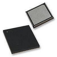
PIC16F1947-E/MR Microchip Technology, PIC16F1947-E/MR Datasheet - Page 3

PIC16F1947-E/MR
Manufacturer Part Number
PIC16F1947-E/MR
Description
28KB Flash, 1KB RAM, 256B EEPROM, LCD, 1.8-5.5V 64 QFN 9x9x0.9mm TUBE
Manufacturer
Microchip Technology
Series
PIC® XLP™ 16Fr
Datasheets
1.PIC16F722-ISS.pdf
(8 pages)
2.PIC16LF1933-ISS.pdf
(46 pages)
3.PIC16LF1946-IPT.pdf
(448 pages)
4.PIC16LF1946-IPT.pdf
(6 pages)
5.PIC16F1946-IPT.pdf
(8 pages)
Specifications of PIC16F1947-E/MR
Core Processor
PIC
Core Size
8-Bit
Speed
32MHz
Connectivity
I²C, LIN, SPI, UART/USART
Peripherals
Brown-out Detect/Reset, LCD, POR, PWM, WDT
Number Of I /o
54
Program Memory Size
28KB (16K x 14)
Program Memory Type
FLASH
Eeprom Size
256 x 8
Ram Size
1K x 8
Voltage - Supply (vcc/vdd)
1.8 V ~ 5.5 V
Data Converters
A/D 17x10b
Oscillator Type
Internal
Operating Temperature
-40°C ~ 125°C
Package / Case
64-VQFN Exposed Pad, 64-HVQFN, 64-SQFN, 64-DHVQFN
Processor Series
PIC16F
Core
PIC
Data Bus Width
8 bit
Data Ram Size
1 KB
Interface Type
MI2C, SPI, EUSART
Maximum Clock Frequency
32 MHz
Number Of Programmable I/os
54
Number Of Timers
5
Operating Supply Voltage
1.8 V to 5.5 V
Maximum Operating Temperature
+ 125 C
Mounting Style
SMD/SMT
3rd Party Development Tools
52715-96, 52716-328, 52717-734
Development Tools By Supplier
PG164130, DV164035, DV244005, DV164005
Minimum Operating Temperature
- 40 C
On-chip Adc
10 bit, 17 Channel
On-chip Dac
5 bit
Lead Free Status / RoHS Status
Lead free / RoHS Compliant
Lead Free Status / RoHS Status
Lead free / RoHS Compliant
Silicon Errata Issues
1. Module: Oscillator
1.1 HS Oscillator
FIGURE 1:
2010 Microchip Technology Inc.
Note:
F
T
T
See the ADC Clock Period (T
section of the DS41414B data sheet.
The HS oscillator requires a minimum voltage of
3.0 volts (at 65°C or less) to operate at 20 MHz.
Work around
None.
Affected Silicon Revisions
CY
AD
OSC
A2
X
= 4/32 MHz = 125 nsec
= 1 µsec, ADCS = F
= 32 MHz
This document summarizes all silicon
errata issues from all revisions of silicon,
previous as well as current. Only the
issues indicated by the shaded column in
the following tables apply to the current
silicon revision (A4).
4 T
A3
8 T
1 T
CY
CY
AD
A4
INSTRUCTION CYCLE DELAY CALCULATION EXAMPLE
OSC
/32
AD
) vs. Device Operating Frequencies table, in the Analog-to-Digital Converter
88 T
11 T
84 T
CY
AD
CY
2. Module: ADC
2.1 Analog-to-Digital Converter (ADC)
PIC16(L)F1946/1947
Under certain device operating conditions, the
ADC conversion may not complete properly. When
this occurs, the ADC Interrupt Flag (ADIF) does
not get set, the ADGO/DONE bit does not get
cleared and the conversion result does not get
loaded into the ADRESH and ADRESL result reg-
isters.
Work around
Method 1: Select
Method 2: Provide a fixed delay in software
oscillator as the ADC conversion
clock source, and perform all
conversions with the device in
Sleep.
to stop the A-to-D conversion
manually, after all 10 bits are
converted,
conversion
automatically. The conversion is
stopped by clearing the GO/
DONE bit in software. The GO/
DONE bit must be cleared during
the last ½ T
conversion
completed automatically. Refer to
Figure 1
Stop the A/D conversion
between 10.5 and 11 T
cycles.
See the Analog-to-Digital
Conversion Timing diagram
in
Converter section of the
DS41414B data sheet.
the
for details.
the
AD
Analog-to-Digital
but
would
cycle, before the
DS80497C-page 3
dedicated
would
before
complete
AD
have
RC
the


