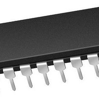
PIC16F1829-E/P Microchip Technology, PIC16F1829-E/P Datasheet - Page 115

PIC16F1829-E/P
Manufacturer Part Number
PIC16F1829-E/P
Description
14 KB Flash, 1K Bytes RAM, 32 MHz Int. Osc, 18 I/0, Enhanced Mid Range Core 20 P
Manufacturer
Microchip Technology
Series
PIC® XLP™ mTouch™ 16Fr
Datasheet
1.PIC16LF1829-ISO.pdf
(420 pages)
Specifications of PIC16F1829-E/P
Core Processor
PIC
Core Size
8-Bit
Speed
32MHz
Connectivity
I²C, LIN, SPI, UART/USART
Peripherals
Brown-out Detect/Reset, POR, PWM, WDT
Number Of I /o
17
Program Memory Size
14KB (8K x 14)
Program Memory Type
FLASH
Eeprom Size
256 x 8
Ram Size
1K x 8
Voltage - Supply (vcc/vdd)
1.8 V ~ 5.5 V
Data Converters
A/D 12x10b
Oscillator Type
Internal
Operating Temperature
-40°C ~ 125°C
Package / Case
*
Processor Series
PIC16F182x
Core
PIC
Data Bus Width
8 bit
Data Ram Size
1 KB
Interface Type
I2C, SPI, USART
Maximum Clock Frequency
32 MHz
Number Of Programmable I/os
18
Number Of Timers
5
Operating Supply Voltage
1.8 V to 5.5 V
Maximum Operating Temperature
+ 125 C
Mounting Style
Through Hole
Lead Free Status / RoHS Status
Lead free / RoHS Compliant
Lead Free Status / RoHS Status
Lead free / RoHS Compliant
- Current page: 115 of 420
- Download datasheet (5Mb)
After the “BSF EECON1,WR” instruction, the processor
requires two cycles to set up the write operation. The
user must place two NOP instructions after the WR bit is
set. The processor will halt internal operations for the
typical 2 ms, only during the cycle in which the write
takes place (i.e., the last word of the block write). This
is not Sleep mode as the clocks and peripherals will
FIGURE 11-2:
2010 Microchip Technology Inc.
EEADRL<4:0> = 00000
First word of block
to be written
Buffer Register
BLOCK WRITES TO FLASH PROGRAM MEMORY WITH 32 WRITE LATCHES
14
EEADRL<4:0> = 00001
7
Buffer Register
5
EEDATH
Preliminary
6
14
Program Memory
EEADRL<4:0> = 00010
0 7
continue to run. The processor does not stall when
LWLO = 1, loading the write latches. After the write
cycle, the processor will resume operation with the third
instruction after the EECON1 write instruction.
PIC16F/LF1825/1829
EEDATA
Buffer Register
8
14
EEADRL<4:0> = 11111
0
Buffer Register
Last word of block
DS41440A-page 115
to be written
14
Related parts for PIC16F1829-E/P
Image
Part Number
Description
Manufacturer
Datasheet
Request
R

Part Number:
Description:
IC, 8BIT MCU, PIC16F, 32MHZ, SOIC-18
Manufacturer:
Microchip Technology
Datasheet:

Part Number:
Description:
IC, 8BIT MCU, PIC16F, 32MHZ, SSOP-20
Manufacturer:
Microchip Technology
Datasheet:

Part Number:
Description:
IC, 8BIT MCU, PIC16F, 32MHZ, DIP-18
Manufacturer:
Microchip Technology
Datasheet:

Part Number:
Description:
IC, 8BIT MCU, PIC16F, 32MHZ, QFN-28
Manufacturer:
Microchip Technology
Datasheet:

Part Number:
Description:
IC, 8BIT MCU, PIC16F, 32MHZ, QFN-28
Manufacturer:
Microchip Technology
Datasheet:

Part Number:
Description:
IC, 8BIT MCU, PIC16F, 32MHZ, QFN-28
Manufacturer:
Microchip Technology
Datasheet:

Part Number:
Description:
IC, 8BIT MCU, PIC16F, 32MHZ, SSOP-20
Manufacturer:
Microchip Technology
Datasheet:

Part Number:
Description:
IC, 8BIT MCU, PIC16F, 20MHZ, DIP-40
Manufacturer:
Microchip Technology
Datasheet:

Part Number:
Description:
IC, 8BIT MCU, PIC16F, 32MHZ, QFN-28
Manufacturer:
Microchip Technology
Datasheet:

Part Number:
Description:
IC, 8BIT MCU, PIC16F, 20MHZ, MQFP-44
Manufacturer:
Microchip Technology
Datasheet:

Part Number:
Description:
IC, 8BIT MCU, PIC16F, 20MHZ, QFN-20
Manufacturer:
Microchip Technology
Datasheet:

Part Number:
Description:
IC, 8BIT MCU, PIC16F, 32MHZ, QFN-28
Manufacturer:
Microchip Technology
Datasheet:

Part Number:
Description:
MCU 14KB FLASH 768B RAM 64-TQFP
Manufacturer:
Microchip Technology
Datasheet:

Part Number:
Description:
7 KB Flash, 384 Bytes RAM, 32 MHz Int. Osc, 16 I/0, Enhanced Mid Range Core, Low
Manufacturer:
Microchip Technology

Part Number:
Description:
14KB Flash, 512B RAM, 256B EEPROM, LCD, 1.8-5.5V 40 UQFN 5x5x0.5mm TUBE
Manufacturer:
Microchip Technology
Datasheet:


